


RP402 Series
PWM/VFM Step-up DC/DC Converter with Synchronous Rectifier


Description
The RP402 Series are min. 0.6V input, CMOS-based PWM/VFM step-up DC/DC converters with synchronous rectifier. The RP402 have three switching control types, or PWM control, forced PWM control, and PWM/VFM auto change control. The RP402 includes a soft start circuit, a bypass switch, shutdown switch, an anti-ringing switch. By simply using with an inductor, a capacitor, and resistors (for output voltage adjustable type) as external components, a high-efficiency step-up DC/DC converter can be realized. The output voltage can be selected from the internally fixed type or externally adjustment is possible. In addition to SOT-23-5 package, a 2.0mm square DFN(PL)2020-8 package is available. The RP402 are ideal for the applications powered by one-cell or two-cell alkaline, nickel-metal-hydride (NiMH) or one-cell Lithium-ion (Li+) batteries.
Spec
| Standard | |
|---|---|
| Input Voltage Range | Internally Fixed Ver.: 0.6 V to 4.8 V Externally Adjustable Ver: 0.6 V to 4.6 V |
| Operating Temperature Range | -40°C to 85°C (125°C) |
| Supply Current | Typ. 21 µA |
| Standby Current | Typ. 0.2 µA |
| Start-up Voltage | Typ. 0.7 V |
| Output Voltage Range | 1.8 V to 5.5 V Internally Fixed Ver.(Except RP402K00xx): 0.1 V step Externally Adjustable (RP402K00xx) |
| Output Voltage Accuracy | ±1.5% |
| Feedback Voltage | 1.0 V |
| Feedback Voltage Accuracy | ±15 mV |
| Output Current | 800 mA (VIN = 3.6 V, VOUT = 5.0 V) |
| Driver ON-resistance | NMOS/ PMOS: 0.20 Ω (VOUT = 5.0 V, 25°C) |
| Oscillator Frequency | 1.2 MHz (Normal PWM Type), 1.0 MHz (Forced PWM Type) |
| Efficiency | 94% (100 mA/ 5.0 V, VIN = 3.6 V, 25°C) 90% (1 mA/ 5.0 V, VIN = 3.6 V, 25°C) |
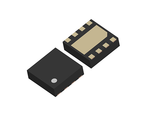
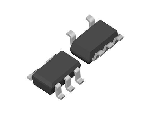
| Package | DFN(PL)2020-8, SOT-23-5 |
Protections / Functions
| TSD | OCP | OVP | UVLO | OVLO | Reverse | Shutdown | Soft Start | SSCG | PGOOD | Auto Discharge | Anti-ringing | Sequencing | Max Duty | Ext. Phase | LED Adjust |
|---|---|---|---|---|---|---|---|---|---|---|---|---|---|---|---|
 |
|
|
|
|
|
Functional Description
| TSD | Thermal Shutdown Function |
|---|---|
| OCP | Overcurrent Protection Note: The function previously labeled as "ILX (LX Current Limit Function)" is now shown as "OCP." |
| OVP | Overvoltage Protection |
| UVLO | Undervoltage Lockout Protection |
| OVLO | Overvoltage Lockout Protection |
| Reverse | Reverse Current Protection Circuit |
| Shutdown | Shutdown Function |
| Soft Start | Soft Start Function |
| SSCG | Spread Spectrum Clock Generator Function |
| PGOOD | Power Good Output |
| Auto Discharge | Auto Discharge Function |
| Anti-ringing | Anti-ringing Switch Function |
| Sequencing | Start-up Sequencing Control |
| Max Duty | Maximum Duty Cycle |
| Ext. Phase | Externally Adjustable Phase Compensation |
| LED Adjust | LED High-speed Dimming Control |
Technical Documents
-
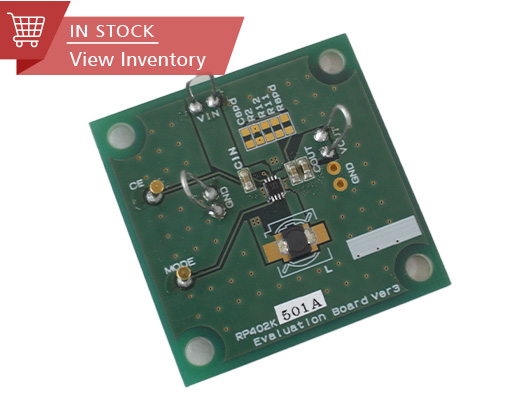
Evaluation Board
-
RP402Kxxxx Typical Application (Adjustable Output Voltage Type)
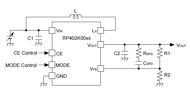
L: 2.2 µH, C1: 10 µF, C2: 10 µF x2
-
RP402K/Nxxxx Typical Application (Fixed Output Voltage Type)
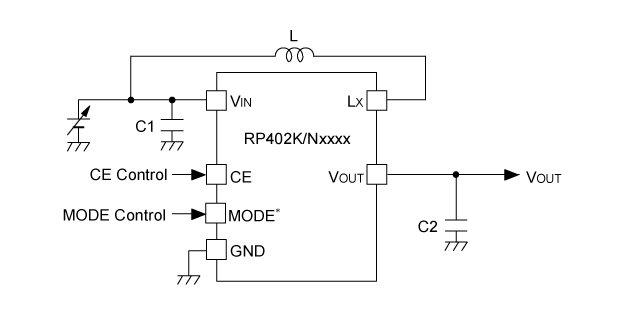
*) MODE pin : only RP402Kxxxx.
L: 2.2 µH, C1: 10 µF, C2: 10 µF x2 -
RP402x501x / RP402K501x (VOUT=5.0V) Efficiency vs. Output Current: Fixed PWM control
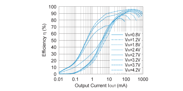
-
RP402x501x / RP402K501x (VOUT=5.0V) Efficiency vs. Output Current: PWM/VFM auto switching control
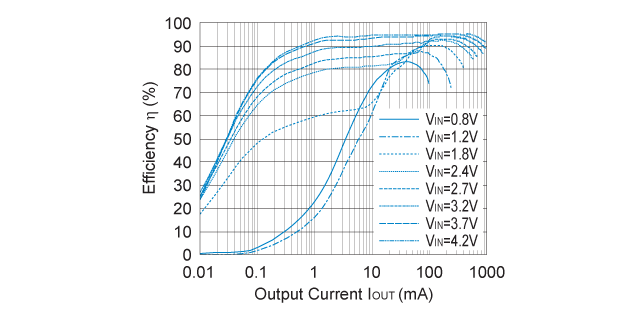
-
Related Links
Quality & Packages

- Refer to the datasheets for the details on the product.
- The package file or the datasheet includes package dimensions, taping specifications, taping reels dimensions, power dissipations, and recommended land pattern.
FAQ
Buy / Contact
-
Purchase, Request for samples and documentsSales are made through distributors. Please contact your local distributors for any sales-related inquiry such as price.
-
Available from 1 piece!Our electronic device products are available through our authorized online distributors.
-
Technical Support