


Foundry Service
-
Kawagoe Plant
As a leading foundry manufacturer for analog and mixed-signal products, Nisshinbo Micro Devices Inc. offers highly reliable process technologies, which are well optimized in our own product development.
The technologies are ranging from 4.0 to 0.35um, and Bipolar, CMOS with HVMOS, high speed BiCMOS, and BCD. Since the technologies are available on 5", and 8" wafers, Nisshinbo Micro Devices can appropriately respond to wide range production volume with our two manufacturing fab and UMC' 8" fab.Leading technologies
ProcessProcess PDF Details Complimentary 40V High Speed Bipolar with TFR
Application : OpAmp126KB 2.0µm rule
NPN ft= 2.9GHz, Vertical PNP ft= 3.7GHz
Wafer Size 5"High Speed BiCMOS
Application : Industrial, Visual, Sensor AFE217KB 0.8μm rule
Bipolar 10V NPN ft= 8.0GHz, Vertical PNP ft= 5.5GHz, CMOS 5V
Wafer Size 5"Analog CMOS+HV
Application : Power Supply, Audio, OpAmp212KB 0.7µm rule
LV 5V, HV 20V/30V/36V
Wafer Size 5"BCD
Application : Power Supply, OpAmp128KB 0.35µm rule
Bipolar 15V NPN, LPNP, CMOS 3.3V/5.0V, DMOS 40V/50V
Wafer Size 8"(*1)Analog CMOS+HV
Application : Power Supply, OpAmpPlease contact us. 0.35µm rule
LV 3.3V, MV 5.0V, HV 12~36V
Wafer Size 8"(*1)(*1):This process was developed in cooperation with UMC.
Inspection items on foundry service
- Process control monitor (Device characteristics)
- Appearance defects
Optional services
- Wafer sort
- Final Test
- Package
Product forms
The PCM data is attached to the product at delivery.
- Wafer
- Bare die
Business flow
The standard business flow of foundry service is as follows.
If you have any questions,please contuct us.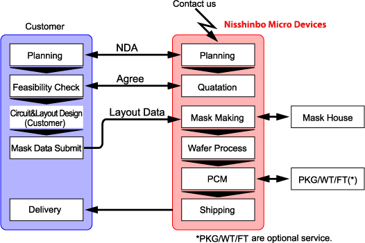
Contacts
Thank you for your visit to our Foundry Service web site. Please click on the "contact" button.
-
Nisshinbo Micro Devices Fukuoka
As a leading foundry manufacturer for analog and mixed-signal products, Nisshinbo Micro Devices Fukuoka Co., Ltd. offers highly reliable process technologies, which are well optimized in our own product development.
The technologies are ranging from 4.0 to 2.0um, and Bipolar process. Since the technologies are available on 5", and 6" wafers.Leading technologies
ProcessProcess PDF Details 40V Bipolar
Application : OpAmp69KB 3.0µm rule
NPN ft= 0.69GHz, Lateral PNP ft= 5.85MHz
Wafer Size 5"40V Bipolar with VPNP (Under development)
Application : OpAmp (Scheduled to be developed)69KB 3.0µm rule
Wafer Size 6"9V Bipolar with VPNP
Application : Industrial, Information43KB 2.0µm rule
NPN ft= 6GHz, Vertical PNP ft= 1.5GHz
Wafer Size 5"40V Bipolar with VPNP
Application : Industrial43KB 2.0µm rule
NPN ft= 2GHz, Vertical PNP ft= 80MHz
Wafer Size 5"Inspection items on foundry service
- Process control monitor (Device characteristics)
- Appearance defects
Optional services
- Wafer sort
- Final Test
- Package
Product forms
The PCM data is attached to the product at delivery.
- Wafer
- Bare die
Business flow
The standard business flow of foundry service is as follows.
If you have any questions,please contuct us.Contacts
Thank you for your visit to our Foundry Service web site. Please click on the "contact" button.
-
Yashiro Plant
We offer Wafer Foundry Services of 150mm and 200mm process, by using CMOS analog processes cultivated by based on our own analog products. We would modify our analog processes according to customers' requirements flexibly. Please feel free to contact us.
Technology: CMOS analog processes
Nisshinbo Micro Devices' manufacturing service offers the following basic processes with Design Rules and Spice Parameters, including TEG's for the evaluation of Analog Characteristics.
Process & OptionsFeature / Prosess 0.8 µm 0.6 µm 0.5 µm 0.35 µm Max. Operating Voltage for LV core Tr. 6.0 V 6.0 V 3.6 V / 6.5 V 3.3 V / 5.0 V / 6.5 V Multi Vth (Low , Dep) 16 V Transistor Option 20 V Transistor Option 30 V Transistor Option 40 V Transistor Option 50 V Transistor Option OTP/ E2PROM BJT: Vertical/Lateral PNP VPNP VPNP Triple Well Thin Film Resister TBA High Resistivity Polysilicon Low TC Resistor Depletion Capacitor PiP Capacitor Laser Fuse Technology Number of Metal Layers 2 3 3 4 Buffer Coat (PBO) Thick Metal Interconnect