RP402 系列
带同步整流器功能的PWM/VFM升压DC/DC转换器


概述
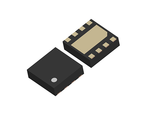
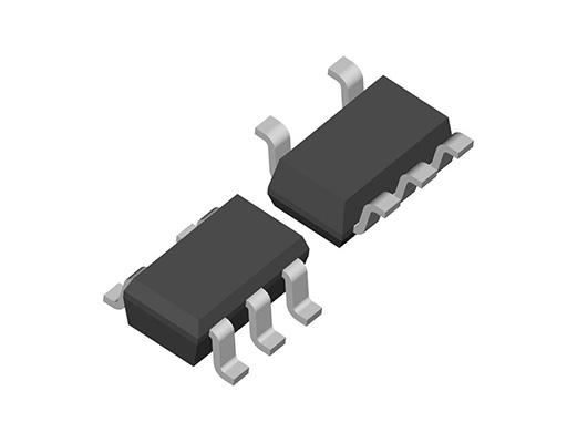
The RP402 Series are min. 0.6V input, CMOS-based PWM/VFM step-up DC/DC converters with synchronous rectifier. The RP402 have three switching control types, or PWM control, forced PWM control, and PWM/VFM auto change control. The RP402 includes a soft start circuit, a bypass switch, shutdown switch, an anti-ringing switch. By simply using with an inductor, a capacitor, and resistors (for output voltage adjustable type) as external components, a high-efficiency step-up DC/DC converter can be realized. The output voltage can be selected from the internally fixed type or externally adjustment is possible. In addition to SOT-23-5 package, a 2.0mm square DFN(PL)2020-8 package is available. The RP402 are ideal for the applications powered by one-cell or two-cell alkaline, nickel-metal-hydride (NiMH) or one-cell Lithium-ion (Li+) batteries.
规格
| 消费 | |
|---|---|
| 输入电压范围 | Internally Fixed Ver.: 0.6 V to 4.8 V Externally Adjustable Ver: 0.6 V to 4.6 V |
| 工作温度范围 | -40°C to 85°C (125°C) |
| 电源电流 | Typ. 21 µA |
| 待机电流 | Typ. 0.2 µA |
| 启动电压 | Typ. 0.7 V |
| 输出电压范围 | 1.8 V to 5.5 V Internally Fixed Ver.(Except RP402K00xx): 0.1 V step Externally Adjustable (RP402K00xx) |
| 输出电压精度 | ±1.5% |
| 反馈电压 | 1.0 V |
| 反馈电压精度 | ±15 mV |
| 输出电流 | 800 mA (VIN = 3.6 V, VOUT = 5.0 V) |
| 驱动器导通电阻 | NMOS/ PMOS: 0.20 Ω (VOUT = 5.0 V, 25°C) |
| 振荡器频率 | 1.2 MHz (Normal PWM Type), 1.0 MHz (Forced PWM Type) |
| 效率 | 94% (100 mA/ 5.0 V, VIN = 3.6 V, 25°C) 90% (1 mA/ 5.0 V, VIN = 3.6 V, 25°C) |
| 封装 | DFN(PL)2020-8, SOT-23-5 |
保护回路/功能
| TSD | OCP | OVP | UVLO | OVLO | Reverse | Shutdown | Soft Start | SSCG | PGOOD | Auto Discharge | Anti-ringing | Sequencing | Max Duty | Ext. Phase | LED Adjust |
|---|---|---|---|---|---|---|---|---|---|---|---|---|---|---|---|
 |
|
|
|
|
|
功能说明
| TSD | 热关断电路 |
|---|---|
| OCP | 过流保护 注:以前标记为“ILX”的功能现在改为“OCP”。 |
| OVP | 过压保护 |
| UVLO | 欠压锁定功能 |
| OVLO | Overvoltage Lockout Protection |
| Reverse | 反向电流保护电路 |
| Shutdown | 关机功能 |
| Soft Start | 软启动功能 |
| SSCG | Spread Spectrum Clock Generator Function |
| PGOOD | Power Good Output |
| Auto Discharge | 自动放电功能 |
| Anti-ringing | Anti-ringing Switch Function |
| Sequencing | Start-up Sequencing Control |
| Max Duty | 最大占空比 |
| Ext. Phase | 外部可调相位补偿 |
| LED Adjust | LED High-speed Dimming Control |
技术资料
-
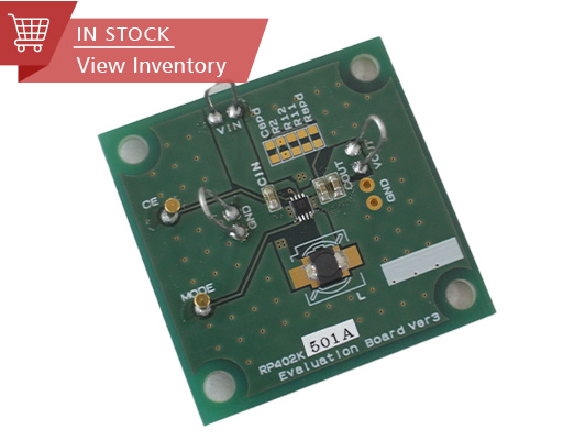
Evaluation Board
-
RP402Kxxxx Typical Application (Adjustable Output Voltage Type)
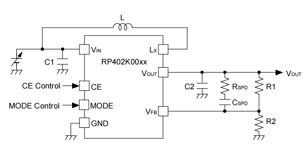
L: 2.2 µH, C1: 10 µF, C2: 10 µF x2
-
RP402K/Nxxxx Typical Application (Fixed Output Voltage Type)
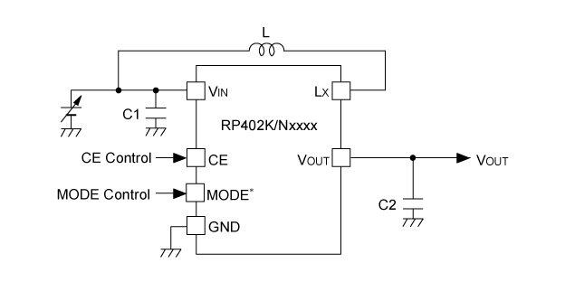
*) MODE pin : only RP402Kxxxx.
L: 2.2 µH, C1: 10 µF, C2: 10 µF x2 -
RP402x501x / RP402K501x (VOUT=5.0V) Efficiency vs. Output Current: Fixed PWM control
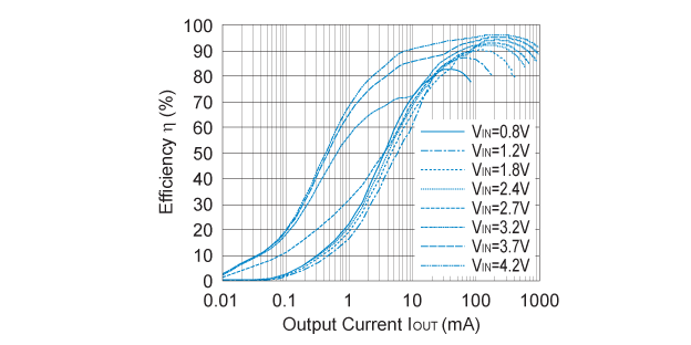
-
RP402x501x / RP402K501x (VOUT=5.0V) Efficiency vs. Output Current: PWM/VFM auto switching control
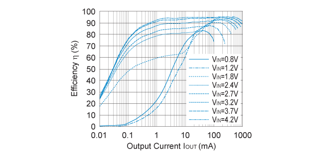
-
相关信息
品质・封装

- 有关产品的详细信息,请参见数据表。
- 封装文件或数据表包括封装尺寸,卷带规格,卷带盘尺寸,功耗和建议的焊盘图案。
常问问题
购买 / 联系我们
-
技术支持