


RP512 Series
0.3µA IQ Low Quiescent Current 300mA Buck DC/DC Converter with Synchronous Rectifier
RP512 Series
0.3µA IQ Low Quiescent Current 300mA Buck DC/DC Converter with Synchronous Rectifier
- Download Datasheet
- Point
-
Provides at-a-glance product features, functions, and concepts.
- ECAD Model: Learn more
-


拡大
:q
:q
:q
Description
RP512 is a buck DCDC converter featuring 0.3 µA ultra-low operating quiescent current. It is suitable for use in wearable and IoT devices that require miniaturization and long-lifetime of battery.
Key Benefits
- VFM (fSW up to 1 MHz) control achieves 0.3 µA ultra-low operating quiescent current.
- The wide range of VIN from 2.0 V to 5.5 V allows operation from coin cell to USB port.
- Total mount area including CIN, COUT, and inductor is 10.6 mm2.
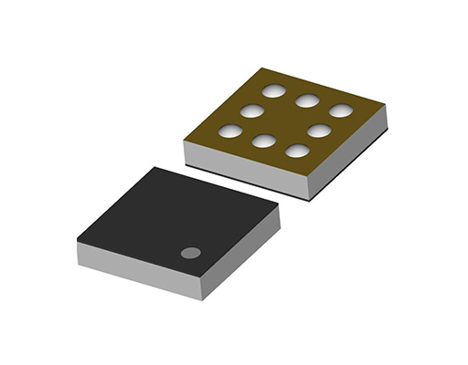
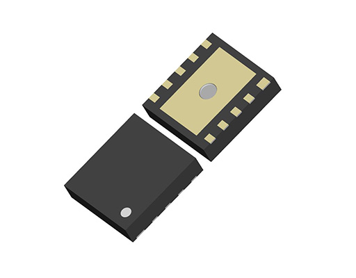
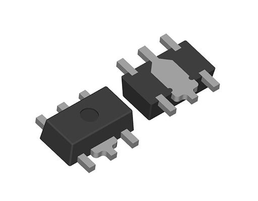
- Selectable packages including WLCSP, DFN, and SOT. 0.4 mm-thickness WLCSP package adaptable to IC cards.
Spec
| Standard | |
|---|---|
| Input Voltage Range | 2.0 V to 5.5 V (6.5 V) |
| Operating Temperature Range | -40°C to 85°C (125°C) |
| Standby Current | Typ. 0.01 µA |
| Operating Quiescent Current | Typ. 0.3 µA |
| Output Voltage Range | 1.0 V to 4.0 V (0.1 V step) |
| Output Voltage Accuracy | ±1.5% (VSET ≥ 1.2 V, Ta = 25°C) ±18 mV (VSET < 1.2 V) |
| Output Current | 300 mA |
| Driver ON-resistance | PMOS: Typ. 0.15 Ω, NMOS: Typ. 0.15 Ω (RP512Z) |
| Oscillator Frequency | 1 MHz |
| Package | WLCSP-8-P1, DFN(PL)2527-10, SOT-89-5 |
Protections / Functions
| TSD | OCP | OVP | UVLO | OVLO | Reverse | Shutdown | Soft Start | SSCG | PGOOD | Auto Discharge | Anti-ringing | Sequencing | Max Duty | Ext. Phase | LED Adjust |
|---|---|---|---|---|---|---|---|---|---|---|---|---|---|---|---|
 |
|
|
|
Functional Description
| TSD | Thermal Shutdown Function |
|---|---|
| OCP | Overcurrent Protection Note: The function previously labeled as "ILX (LX Current Limit Function)" is now shown as "OCP." |
| OVP | Overvoltage Protection |
| UVLO | Undervoltage Lockout Protection |
| OVLO | Overvoltage Lockout Protection |
| Reverse | Reverse Current Protection Circuit |
| Shutdown | Shutdown Function |
| Soft Start | Soft Start Function |
| SSCG | Spread Spectrum Clock Generator Function |
| PGOOD | Power Good Output |
| Auto Discharge | Auto Discharge Function |
| Anti-ringing | Anti-ringing Switch Function |
| Sequencing | Start-up Sequencing Control |
| Max Duty | Maximum Duty Cycle |
| Ext. Phase | Externally Adjustable Phase Compensation |
| LED Adjust | LED High-speed Dimming Control |
Technical Documents
-
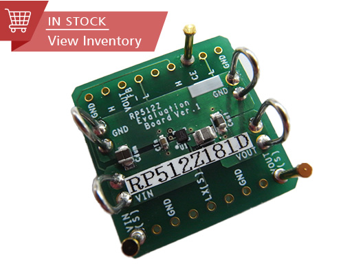
Evaluation Board
Evaluation Board Datasheet Inventory RP512Z181D-EV Datasheet -
Typical Application
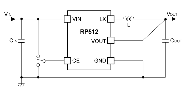
L: 2.2 µH, CIN: 10 µF, COUT: 22 µF
-
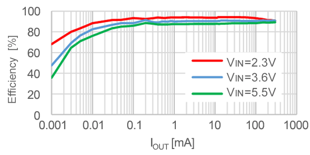
Efficiency vs. Output Current (VOUT = 1.8 V)
-
Related Links
Quality & Packages
| Product Name | Compatibility | Package | Marking | Reliability |
|---|---|---|---|---|
| RP512Zxx1x-TR-T |
|
WLCSP-8-P1 | See datasheet | RP512Z-T |
| RP512Kxx1x-TR |
|
DFN(PL)2527-10 | See datasheet | RP512K |
| RP512Hxx1x-T1-FE |
|
SOT-89-5 | See datasheet | RP512H-FE |

- Refer to the datasheets for the details on the product.
- The package file or the datasheet includes package dimensions, taping specifications, taping reels dimensions, power dissipations, and recommended land pattern.
FAQ
Buy / Contact
-
Purchase, Request for samples and documentsSales are made through distributors. Please contact your local distributors for any sales-related inquiry such as price.
-
Available from 1 piece!Our electronic device products are available through our authorized online distributors.
-
Technical Support
RP512 Series