RP512 系列
0.3µA IQ 低静态电流 300mA带同步整流器功能的降压DC/DC转换器
RP512 系列
0.3µA IQ 低静态电流 300mA带同步整流器功能的降压DC/DC转换器


拡大
:q
:q
:q
概述
RP512 is a buck DCDC converter featuring 0.3 µA ultra-low operating quiescent current. It is suitable for use in wearable and IoT devices that require miniaturization and long-lifetime of battery.
特点
- VFM (fSW up to 1 MHz) control achieves 0.3 µA ultra-low operating quiescent current.
- The wide range of VIN from 2.0 V to 5.5 V allows operation from coin cell to USB port.
- Total mount area including CIN, COUT, and inductor is 10.6 mm2.
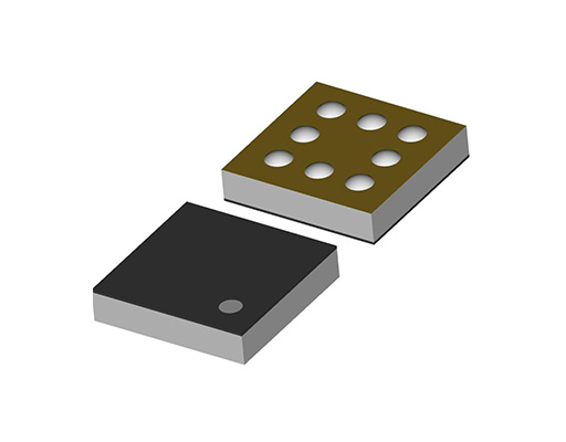
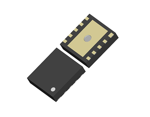
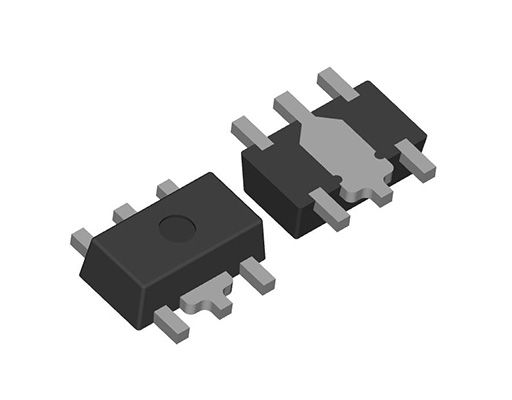
- Selectable packages including WLCSP, DFN, and SOT. 0.4 mm-thickness WLCSP package adaptable to IC cards.
规格
| 消费 | |
|---|---|
| 输入电压范围 | 2.0 V to 5.5 V (6.5 V) |
| 工作温度范围 | -40°C to 85°C (125°C) |
| 待机电流 | Typ. 0.01 µA |
| 工作静态电流 | Typ. 0.3 µA |
| 输出电压范围 | 1.0 V to 4.0 V (0.1 V step) |
| 输出电压精度 | ±1.5% (VSET ≥ 1.2 V, Ta = 25°C) ±18 mV (VSET < 1.2 V) |
| 输出电流 | 300 mA |
| 驱动器导通电阻 | PMOS: Typ. 0.15 Ω, NMOS: Typ. 0.15 Ω (RP512Z) |
| 振荡器频率 | 1 MHz |
| 封装 | WLCSP-8-P1, DFN(PL)2527-10, SOT-89-5 |
保护回路/功能
| TSD | OCP | OVP | UVLO | OVLO | Reverse | Shutdown | Soft Start | SSCG | PGOOD | Auto Discharge | Anti-ringing | Sequencing | Max Duty | Ext. Phase | LED Adjust |
|---|---|---|---|---|---|---|---|---|---|---|---|---|---|---|---|
 |
|
|
|
功能说明
| TSD | 热关断电路 |
|---|---|
| OCP | 过流保护 注:以前标记为“ILX”的功能现在改为“OCP”。 |
| OVP | 过压保护 |
| UVLO | 欠压锁定功能 |
| OVLO | Overvoltage Lockout Protection |
| Reverse | 反向电流保护电路 |
| Shutdown | 关机功能 |
| Soft Start | 软启动功能 |
| SSCG | Spread Spectrum Clock Generator Function |
| PGOOD | Power Good Output |
| Auto Discharge | 自动放电功能 |
| Anti-ringing | Anti-ringing Switch Function |
| Sequencing | Start-up Sequencing Control |
| Max Duty | 最大占空比 |
| Ext. Phase | 外部可调相位补偿 |
| LED Adjust | LED High-speed Dimming Control |
技术资料
-
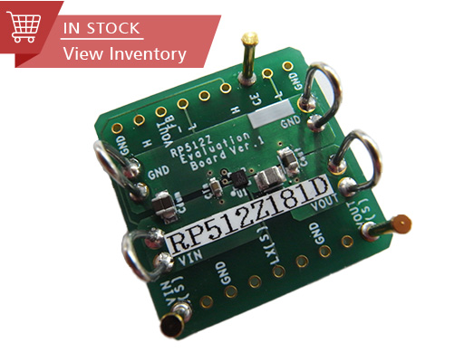
Evaluation Board
Evaluation Board Datasheet Inventory RP512Z181D-EV Datasheet -
Typical Application
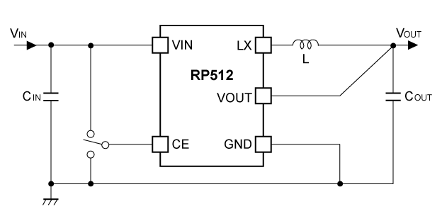
L: 2.2 µH, CIN: 10 µF, COUT: 22 µF
-
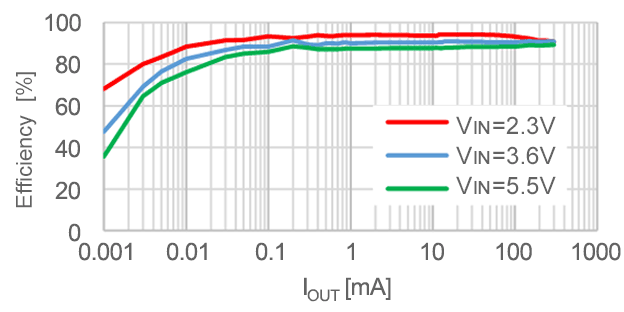
Efficiency vs. Output Current (VOUT = 1.8 V)
-
相关信息
品质・封装
| 产品名称 | 对应 | 封装 | 标注 | 信赖性 |
|---|---|---|---|---|
| RP512Zxx1x-TR-T |
|
WLCSP-8-P1 | 请参见数据表 | RP512Z-T |
| RP512Kxx1x-TR |
|
DFN(PL)2527-10 | 请参见数据表 | RP512K |
| RP512Hxx1x-T1-FE |
|
SOT-89-5 | 请参见数据表 | RP512H-FE |

- 有关产品的详细信息,请参见数据表。
- 封装文件或数据表包括封装尺寸,卷带规格,卷带盘尺寸,功耗和建议的焊盘图案。
常问问题
购买 / 联系我们
-
技术支持