


RP506 Series
2A PWM/VFM Step-down DC/DC Converter with Synchronous Rectifier


Description
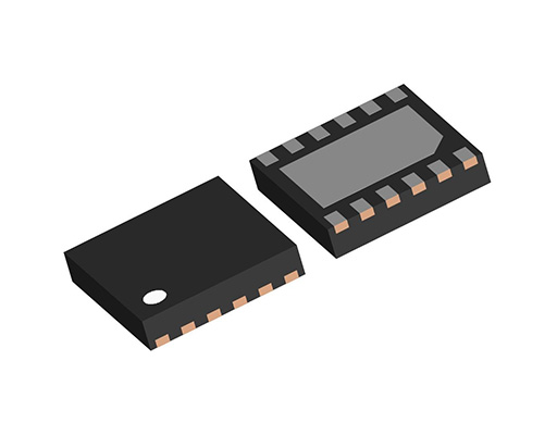
The RP506 Series are low supply current CMOS-based PWM/VFM step-down DC/DC converters with synchronous rectifier. RP506 can be selected from two control types by input signal to the MODE pin - forced PWM control or PWM/VFM auto switching control in which mode automatically switches to high-efficiency VFM mode in low output current. RP506 includes a soft start circuit, an under-voltage lockout circuit (UVLO), thermal shutdown circuit and a latch protection circuit. By simply using an inductor and capacitors (and resistors) as external components, a high-efficiency step-down DC/DC converter can be easily configured. The oscillator frequency can be selected from 1.2MHz, 2.25MHz or 2.3MHz. The soft start time is Typ. 0.15ms, and by connecting an external capacitor to TSS pin, soft start time is adjustable. VOUT/VFB pin voltage is monitored, and the output voltage errors can be output from PG pin. The PG pin is N-channel open drain output type. RP506 is offered in a DFN(PL)2527-10 package for consumer application and a DFN3030-12 package for industrial and automotive applications.
Spec
| Standard | Industrial | Automotive | |
|---|---|---|---|
| Input Voltage Range | 2.5 V to 5.5 V (6.5 V) | ||
| Operating Temperature Range | -40°C to 85°C (125°C) | -40°C to 105°C (125°C) | -40°C to 125°C (150°C) -40°C to 105°C (150°C) |
| Supply Current | Typ. 48 µA(VFM, no load) | ||
| Standby Current | Typ. 0 µA | ||
| Output Voltage Range | Internally Fixed Ver.: 0.6 V to 3.3 V (0.1 V step) Externally Adjustable Ver.: 0.6 V to 4.0 V |
Internally Fixed Ver.: 0.8 V, 1.0 V, 1.1 V, 1.2 V, 1.3 V, 1.5 V, 1.8 V, 1.85 V, 3.0 V, 3.3 V Externally Adjustable Ver.: 0.6 V to 4.0 V |
Internally Fixed Ver.: 0.8 V, 1.0 V, 1.1 V, 1.2 V, 1.3 V, 1.5 V, 1.8 V, 1.85 V, 3.0 V, 3.3 V Externally Adjustable Ver.: 0.6 V to 4.0 V |
| Output Voltage Accuracy | ±1.5% (VSET ≥ 1.2 V , Ta = 25°C) ±18 mV (VSET < 1.2 V) |
||
| Output Voltage Temperature Coefficient | ±100 ppm/°C | ||
| Feedback Voltage Accuracy | ±9 mV (VFB = 0.6 V) | ||
| Feedback Voltage Temperature Coefficient | ±100 ppm/°C | ||
| Output Current | 2 A | ||
| Driver ON-resistance | Pch: Typ. 0.130 Ω, Nch: Typ. 0.125 Ω (VIN = 3.6 V) | ||
| Oscillator Frequency | Typ. 2.25 MHz, 1.2 MHz | Typ. 2.3 MHz, 1.2 MHz | Typ. 2.3 MHz, 1.2 MHz |
| Maximum Duty Cycle | Min. 100% | ||
| Package | DFN(PL)2527-10 | DFN3030-12 | DFN3030-12 |
Protections / Functions
| TSD | OCP | OVP | UVLO | OVLO | Reverse | Shutdown | Soft Start | SSCG | PGOOD | Auto Discharge | Anti-ringing | Sequencing | Max Duty | Ext. Phase | LED Adjust |
|---|---|---|---|---|---|---|---|---|---|---|---|---|---|---|---|
 |
|
|
|
|
|
Functional Description
| TSD | Thermal Shutdown Function |
|---|---|
| OCP | Overcurrent Protection Note: The function previously labeled as "ILX (LX Current Limit Function)" is now shown as "OCP." |
| OVP | Overvoltage Protection |
| UVLO | Undervoltage Lockout Protection |
| OVLO | Overvoltage Lockout Protection |
| Reverse | Reverse Current Protection Circuit |
| Shutdown | Shutdown Function |
| Soft Start | Soft Start Function |
| SSCG | Spread Spectrum Clock Generator Function |
| PGOOD | Power Good Output |
| Auto Discharge | Auto Discharge Function |
| Anti-ringing | Anti-ringing Switch Function |
| Sequencing | Start-up Sequencing Control |
| Max Duty | Maximum Duty Cycle |
| Ext. Phase | Externally Adjustable Phase Compensation |
| LED Adjust | LED High-speed Dimming Control |
Technical Documents
-
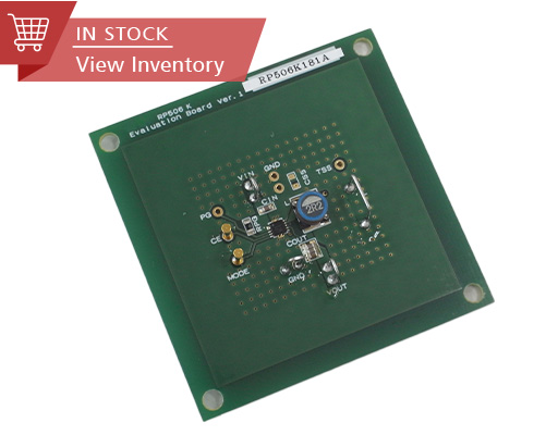
Evaluation Board
Evaluation Board Datasheet Inventory RP506K001F012-EV Datasheet -
Typical Application (Fixed Output Voltage Type)
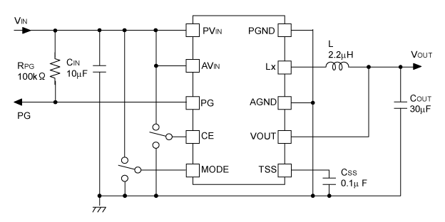
Using Power good function, setting soft- start time for 30ms
-
Typical Application (Adjustable Output Voltage Type)
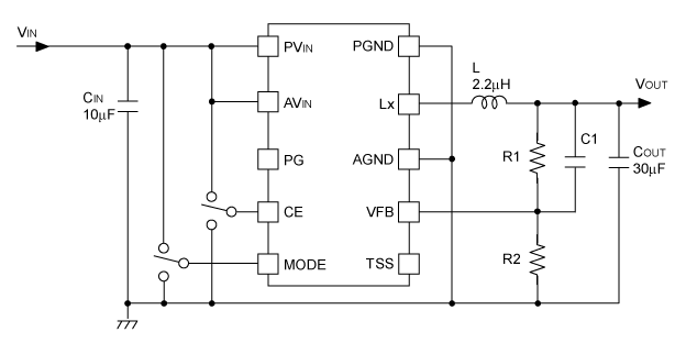
Not using Power good function, setting soft-start time for 0.15ms
-
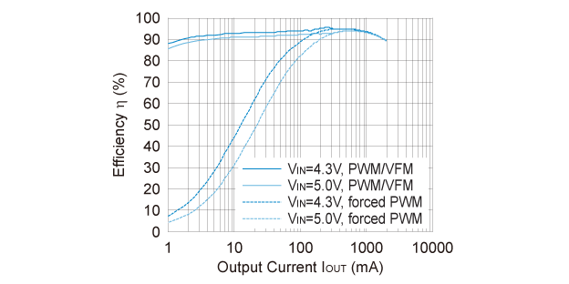
Efficiency vs. Output Current (A/B/C/G/H/N)
-
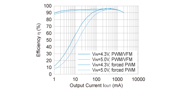
Efficiency vs. Output Current (D/E/F/K/L/M)
-
Related Links
Quality & Packages
| Product Name | Compatibility | Package | Marking | Reliability |
|---|---|---|---|---|
| RP506Kxx1x-TR |
|
DFN(PL)2527-10 | RP506K | RP506K |
| RP506Lxx1x-TR-Y |
|
DFN3030-12 | RP506L | RP506L-Y |
| RP506Lxx1x-TR-K |
|
DFN3030-12 | RP506L | RP506L-K |
| RP506Lxx1x-TR-A |
|
DFN3030-12 | RP506L | RP506L-A |

- Refer to the datasheets for the details on the product.
- The package file or the datasheet includes package dimensions, taping specifications, taping reels dimensions, power dissipations, and recommended land pattern.
Qualification Test Plan (QTP) Sheets
To download the QTP sheets, a myNISD account is required. If you do not have an account, please register in advance.If you already have an account, please click the button below. After logging in to myNISD, the QTP sheet list page for the corresponding series will be displayed.
FAQ
Buy / Contact
-
Purchase, Request for samples and documentsSales are made through distributors. Please contact your local distributors for any sales-related inquiry such as price.
-
Available from 1 piece!Our electronic device products are available through our authorized online distributors.
-
Technical Support