


RP401 Series
1A PWM/VFM Step-up DC/DC Converter


Description
The RP401 Series are CMOS-based PWM/VFM step-up DC/DC converters which can start-up from Typ. 0.6V. RP401 can be switched from two control types by inputting signal to the MODE pin - fixed PWM control or PWM/VFM auto switching control in which mode automatically switches to high-efficiency VFM mode in low output current. (RP401N Series can be selected from fixed PWM control or PWM/VFM auto switching control.) RP401 includes a soft start circuit. By simply using an inductor, a capacitor, (resisters for adjustable type), and a diode as external components, a high-efficiency step-up DC/DC converter can be easily configured. The output voltage can be selected from the internally fixed or the externally adjustment. In addition to SOT-23-5 package, a 1.8mm × 2.0mm square DFN(PL)1820-6 package is also available.
Spec
| Standard | |
|---|---|
| Input Voltage Range | 0.6 V to 5.5 V (6.0 V) |
| Operating Temperature Range | -40°C to 85°C (125°C) |
| Supply Current | Typ. 400 µA (VSET = 3.0 V, switching) Typ. 130 µA (non-switching, VFM mode) Typ. 230 µA (non-switching, PWM mode) |
| Standby Current | Typ. 0.15 µA (CE = "L") |
| Output Voltage Range | 1.8 V to 5.5 V (Internally Fixed: xx1, Externally Adjustable:001) |
| Output Voltage Accuracy | ±2% |
| Feedback Voltage | 0.6 V |
| Feedback Voltage Accuracy | ±2% |
| Oscillator Frequency | Typ. 1.2 MHz |
| Maximum Duty Cycle | Min. 80%, Typ. 88% |
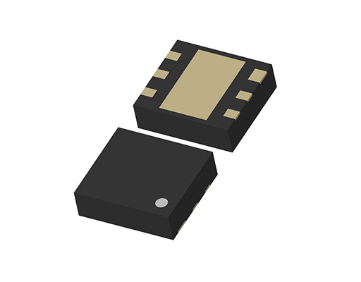
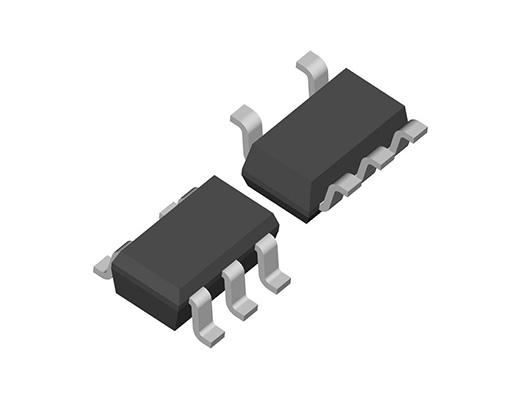
| Package | DFN(PL)1820-6, SOT-23-5 |
Protections / Functions
| TSD | OCP | OVP | UVLO | OVLO | Reverse | Shutdown | Soft Start | SSCG | PGOOD | Auto Discharge | Anti-ringing | Sequencing | Max Duty | Ext. Phase | LED Adjust |
|---|---|---|---|---|---|---|---|---|---|---|---|---|---|---|---|
 |
|
Functional Description
| TSD | Thermal Shutdown Function |
|---|---|
| OCP | Overcurrent Protection Note: The function previously labeled as "ILX (LX Current Limit Function)" is now shown as "OCP." |
| OVP | Overvoltage Protection |
| UVLO | Undervoltage Lockout Protection |
| OVLO | Overvoltage Lockout Protection |
| Reverse | Reverse Current Protection Circuit |
| Shutdown | Shutdown Function |
| Soft Start | Soft Start Function |
| SSCG | Spread Spectrum Clock Generator Function |
| PGOOD | Power Good Output |
| Auto Discharge | Auto Discharge Function |
| Anti-ringing | Anti-ringing Switch Function |
| Sequencing | Start-up Sequencing Control |
| Max Duty | Maximum Duty Cycle |
| Ext. Phase | Externally Adjustable Phase Compensation |
| LED Adjust | LED High-speed Dimming Control |
Technical Documents
-
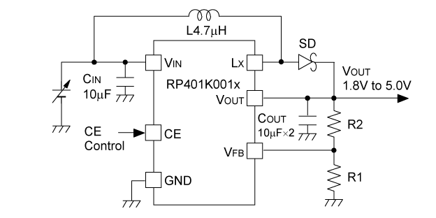
RP401K001C/D Typical Application (Externally adjustable output voltage type)
-
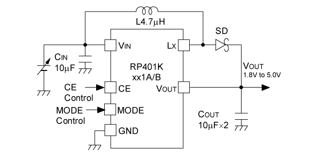
RP401Kxx1A/B Typical Application (Internally fixed output Voltage type)
-
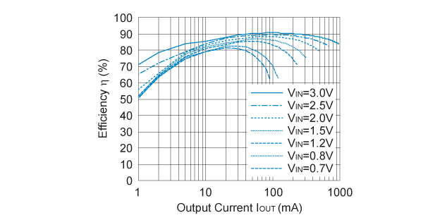
RP401x331x / RP401K001x (VOUT=3.3V) Efficiency vs. Output Current: Fixed PWM control
-
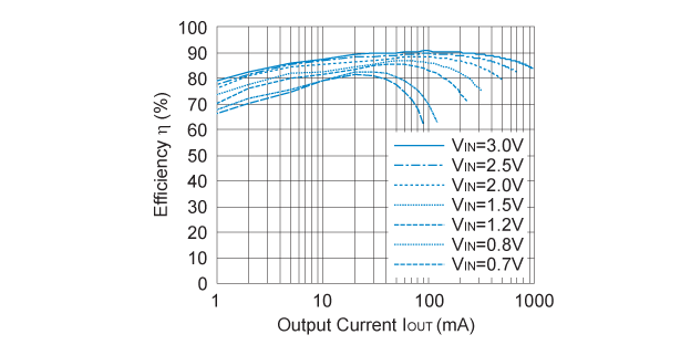
RP401x331x / RP401K001x (VOUT=3.3V) Efficiency vs. Output Current: PWM/VFM auto switching control
-
Related Links
Quality & Packages
| Product Name | Compatibility | Package | Marking | Reliability |
|---|---|---|---|---|
| RP401Kxx1x-TR |
|
DFN(PL)1820-6 | RP401K | RP401K |
| RP401Nxx1x-TR-FE |
|
SOT-23-5 | RP401N | RP401N-FE |

- Refer to the datasheets for the details on the product.
- The package file or the datasheet includes package dimensions, taping specifications, taping reels dimensions, power dissipations, and recommended land pattern.
FAQ
Buy / Contact
-
Purchase, Request for samples and documentsSales are made through distributors. Please contact your local distributors for any sales-related inquiry such as price.
-
Available from 1 piece!Our electronic device products are available through our authorized online distributors.
-
Technical Support