


R1293 Series
Multi Power Supply IC with Amplifier for LCD
R1293 Series
Multi Power Supply IC with Amplifier for LCD


拡大
:q
Description
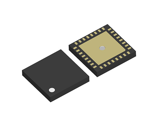
The R1293 is a multi power supply IC dedicated for mid-size TFT LCD panels. The R1293 consists of a PWM control step-up DC/DC converter, an LDO regulator, a VCOM amplifier and six GAMMA amplifiers. The output noise can be reduced by SEL pin. (SEL pin "H": normal mode, SEL pin "L": low noise mode.) The MOSFET for step-up DC/DC converter is built-in and, low power operation is realized by standby mode. The package is 4mm square QFN(PL)0404-32.
Spec
| Standard | |
|---|---|
| Input Voltage Range | DC/DC: 2.2 V to 5.5 V (6.5 V) LDO: 2.2 V to 5.5 V (6.5 V) AMP: 5.0 V to 16 V (24 V) |
| Operating Temperature Range | -40°C to 85°C (125°C) |
| Supply Current | Typ. 300 µA |
| Standby Current | Typ. 60 µA |
| Output Voltage Range | DC/DC: Max. 16 V (Externally Adjustable) LDO: 1.8 V to 2.5 V (Internally Fixed) |
| Output Voltage Accuracy | LDO: ±1.0% |
| Feedback Voltage | DC/DC: 1 V |
| Feedback Voltage Accuracy | DC/DC: ±15 mV |
| Output Current | LDO: 350 mA |
| Oscillator Frequency | Typ. 300 kHz to1 MHz (Externally Adjustable) |
| Maximum Duty Cycle | Typ. 90% (Externally Adjustable) |
| Package | QFN(PL)0404-32 |
| Buffer Amplifier Input Voltage Range | VCOM: 1.5 V to VBUFF -1.5 V GAMMA: 0 V to VBUFF |
| Buffer Amplifier Output Current | VCOM: -100 mA to 100 mA GAMMA: -10 mA to 10 mA |
Protections / Functions
| TSD | OCP | OVP | UVLO | OVLO | Reverse | Shutdown | Soft Start | SSCG | PGOOD | Auto Discharge | Anti-ringing | Sequencing | Max Duty | Ext. Phase | LED Adjust |
|---|---|---|---|---|---|---|---|---|---|---|---|---|---|---|---|
 |
|
|
|
|
|
Functional Description
| TSD | Thermal Shutdown Function |
|---|---|
| OCP | Overcurrent Protection Note: The function previously labeled as "ILX (LX Current Limit Function)" is now shown as "OCP." |
| OVP | Overvoltage Protection |
| UVLO | Undervoltage Lockout Protection |
| OVLO | Overvoltage Lockout Protection |
| Reverse | Reverse Current Protection Circuit |
| Shutdown | Shutdown Function |
| Soft Start | Soft Start Function |
| SSCG | Spread Spectrum Clock Generator Function |
| PGOOD | Power Good Output |
| Auto Discharge | Auto Discharge Function |
| Anti-ringing | Anti-ringing Switch Function |
| Sequencing | Start-up Sequencing Control |
| Max Duty | Maximum Duty Cycle |
| Ext. Phase | Externally Adjustable Phase Compensation |
| LED Adjust | LED High-speed Dimming Control |
Technical Documents
-
Typical Application
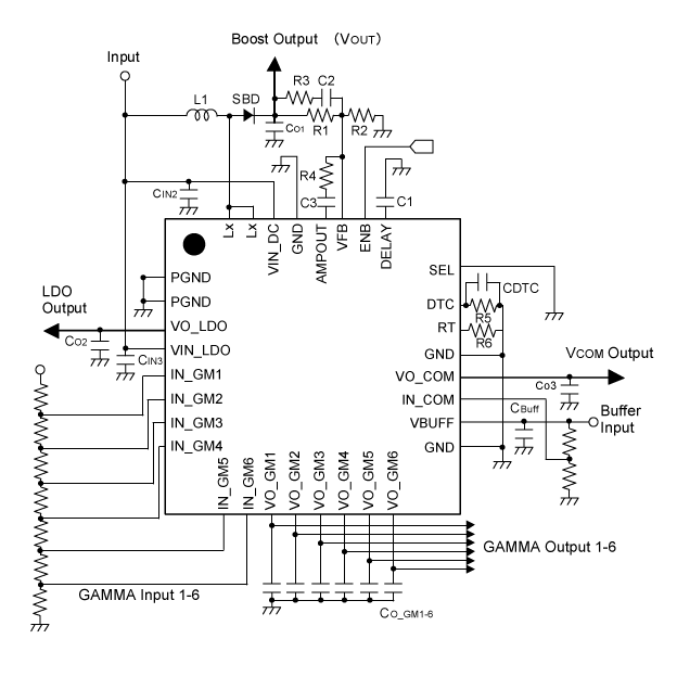
For external parts, please refer to the datasheet. -
Related Links
Quality & Packages
| Product Name | Compatibility | Package | Marking | Reliability |
|---|---|---|---|---|
| R1293Kxx1A-E2 |
|
QFN(PL)0404-32 | R1293K | R1293K |

- Refer to the datasheets for the details on the product.
- The package file or the datasheet includes package dimensions, taping specifications, taping reels dimensions, power dissipations, and recommended land pattern.
FAQ
Buy / Contact
-
Purchase, Request for samples and documentsSales are made through distributors. Please contact your local distributors for any sales-related inquiry such as price.
-
Available from 1 piece!Our electronic device products are available through our authorized online distributors.
-
Technical Support
R1293 Series