


R1225 Series
18.5V Input PWM/VFM Step-down DC/DC Controller


Description
The R1225 Series are low supply current CMOS-based PWM/VFM controlled step-down DC/DC controllers with an external output transistor. By simply using a power transistor, an inductor, a diode, and a capacitor as external components, a high-efficiency step-down DC/DC converter can be easily configured. The PWM/VFM alternative circuit automatically switches to VFM control in the smaller output current range and provides high efficiency even in the smaller output current range. The version with fixed PWM control is also available. The latch type protection circuit embedded into the device latches the power MOS in the "OFF" state when the oscillator maximum duty cycle continues for a predetermined period of time. Protection time is adjustable by the capacity of an external capacitor of the DLY pin. R1225 also includes an under-voltage lockout circuit (UVLO) that stops DC/DC operation and prevents malfunction when the supply voltage falls below the UVLO detector threshold and reduces supply current.
Spec
| Standard | |
|---|---|
| Input Voltage Range | 2.3 V to 18.5 V (20.0 V) |
| Operating Temperature Range | -40°C to 85°C (125°C) |
| Supply Current | Typ. 20 µA (R1225Nxx2A/B/J/K) Typ. 30 µA (R1225Nxx2C) Typ. 40 µA (R1225Nxx2D) |
| Standby Current | Typ. 0 µA |
| Output Voltage Range | 1.2 V to 6.0 V (0.1 V step) |
| Output Voltage Accuracy | ±2% (Ta = 25°C) |
| Output Voltage Temperature Coefficient | Typ. ±100 ppm/°C |
| Oscillator Frequency | Typ. 180 kHz, 300 kHz, 500 kHz |
| Efficiency | Typ. 90% |
| Package | SOT-23-6W |
Protections / Functions
| TSD | OCP | OVP | UVLO | OVLO | Reverse | Shutdown | Soft Start | SSCG | PGOOD | Auto Discharge | Anti-ringing | Sequencing | Max Duty | Ext. Phase | LED Adjust |
|---|---|---|---|---|---|---|---|---|---|---|---|---|---|---|---|
 |
|
|
Functional Description
| TSD | Thermal Shutdown Function |
|---|---|
| OCP | Overcurrent Protection Note: The function previously labeled as "ILX (LX Current Limit Function)" is now shown as "OCP." |
| OVP | Overvoltage Protection |
| UVLO | Undervoltage Lockout Protection |
| OVLO | Overvoltage Lockout Protection |
| Reverse | Reverse Current Protection Circuit |
| Shutdown | Shutdown Function |
| Soft Start | Soft Start Function |
| SSCG | Spread Spectrum Clock Generator Function |
| PGOOD | Power Good Output |
| Auto Discharge | Auto Discharge Function |
| Anti-ringing | Anti-ringing Switch Function |
| Sequencing | Start-up Sequencing Control |
| Max Duty | Maximum Duty Cycle |
| Ext. Phase | Externally Adjustable Phase Compensation |
| LED Adjust | LED High-speed Dimming Control |
Technical Documents
-
R1225Nxx2x Typical Application
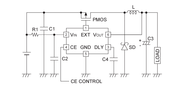
L: 27µH, C1: 10µF, C2: 0.1µF, C3: 47µF, C4: 0.02µF, R1: 10Ω
-
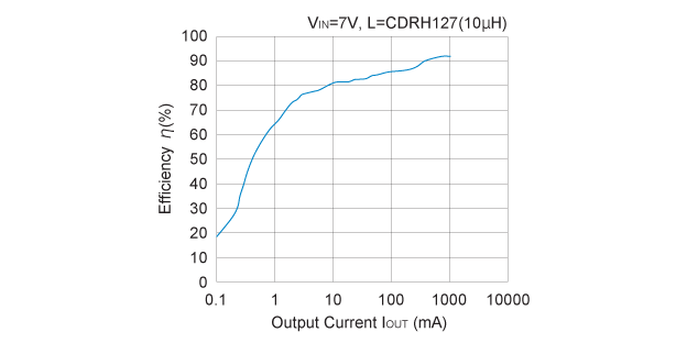
R1225N332A Efficiency vs. Output Current
-
Related Links
Quality & Packages

- Refer to the datasheets for the details on the product.
- The package file or the datasheet includes package dimensions, taping specifications, taping reels dimensions, power dissipations, and recommended land pattern.
FAQ
Buy / Contact
-
Purchase, Request for samples and documentsSales are made through distributors. Please contact your local distributors for any sales-related inquiry such as price.
-
Available from 1 piece!Our electronic device products are available through our authorized online distributors.
-
Technical Support