


R1213 Series
2.5A PWM Step-up DC/DC Converter


Description
The R1213 Series are low supply current, CMOS-based PWM step-up DC/DC converters. R1213 includes a soft start circuit, an under-voltage lockout circuit (UVLO), a thermal shutdown circuit, and a latch protection circuit. By simply using an inductor, resistors, capacitors and a diode as external components, a high-efficiency step-up DC/DC converter can be easily configured. The soft start time as well as phase compensation can be set with external resistors and capacitors. Built-in a shutdown control circuit. It turns off the external Pch MOSFET at the protection time, so it cut off the power line from VDD to VOUT. To release the latch protection, change to the stand-by mode by the CE pin, or change the VDD voltage lower than the UVLO detect voltage.
Spec
| Standard | |
|---|---|
| Input Voltage Range | 2.3 V to 5.5 V (6.5 V) |
| Operating Temperature Range | -40°C to 85°C (125°C) |
| Supply Current | Typ. 550 µA (non-switching) Typ. 3 mA (switching) |
| Standby Current | Typ. 0.1 µA |
| Output Voltage Range | Externally Adjustable: 3.0 V to 15.0 V (VFB = 0.8 V) |
| Feedback Voltage Accuracy | ±8 mV |
| Feedback Voltage Temperature Coefficient | ±50 ppm/°C |
| Output Current | 1.0 A: VIN = 3.3 V, VOUT = 3.8 V 500 mA: VIN = 2.3 V, VOUT = 5.0 V 250 mA: VIN = 2.7 V, VOUT = 9.6 V 150 mA: VIN = 3.0 V, VOUT = 15 V |
| Driver ON-resistance | Typ. 0.07 Ω |
| Oscillator Frequency | Typ. 1.0 MHz |
| Maximum Duty Cycle | Min. 85%, Typ. 90% |
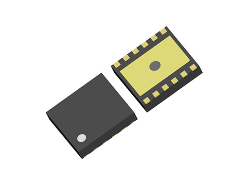
| Package | DFN(PL)2730-12 |
Protections / Functions
| TSD | OCP | OVP | UVLO | OVLO | Reverse | Shutdown | Soft Start | SSCG | PGOOD | Auto Discharge | Anti-ringing | Sequencing | Max Duty | Ext. Phase | LED Adjust |
|---|---|---|---|---|---|---|---|---|---|---|---|---|---|---|---|
 |
|
|
|
|
|
Functional Description
| TSD | Thermal Shutdown Function |
|---|---|
| OCP | Overcurrent Protection Note: The function previously labeled as "ILX (LX Current Limit Function)" is now shown as "OCP." |
| OVP | Overvoltage Protection |
| UVLO | Undervoltage Lockout Protection |
| OVLO | Overvoltage Lockout Protection |
| Reverse | Reverse Current Protection Circuit |
| Shutdown | Shutdown Function |
| Soft Start | Soft Start Function |
| SSCG | Spread Spectrum Clock Generator Function |
| PGOOD | Power Good Output |
| Auto Discharge | Auto Discharge Function |
| Anti-ringing | Anti-ringing Switch Function |
| Sequencing | Start-up Sequencing Control |
| Max Duty | Maximum Duty Cycle |
| Ext. Phase | Externally Adjustable Phase Compensation |
| LED Adjust | LED High-speed Dimming Control |
Technical Documents
-
Download Circuit Module

-
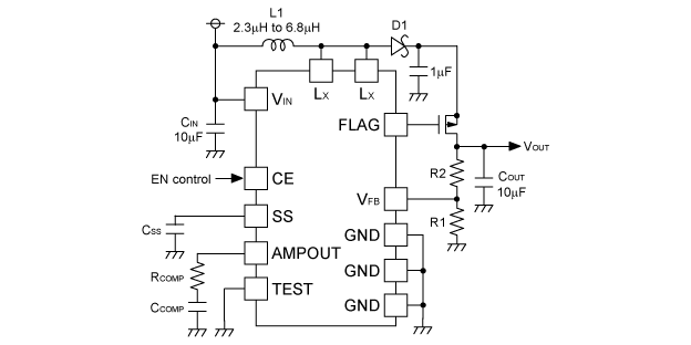
Typical Application (In case of using P-channel MOSEFT for shutdown function)
-
Typical Application (In case of not using shutdown function)
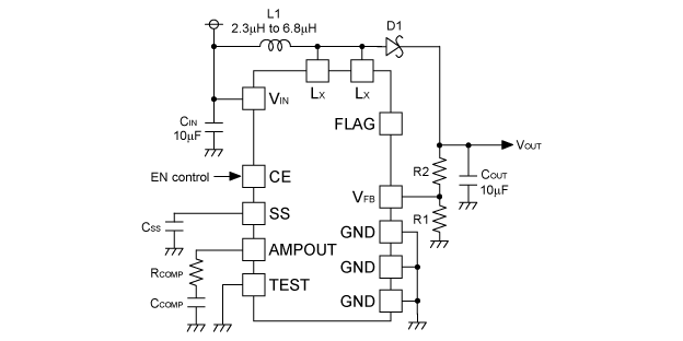
FLAG pin should be open.
-
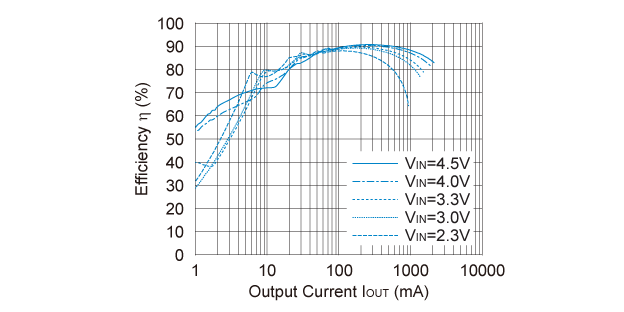
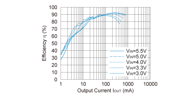
R1213K001A Efficiency vs. Output Current (VOUT=5.0V)
-
R1213K001B Efficiency vs. Output Current (VOUT=15.0V)
-
Related Links
Quality & Packages
| Product Name | Compatibility | Package | Marking | Reliability |
|---|---|---|---|---|
| R1213K001x-TR |
|
DFN(PL)2730-12 | R1213K | R1213K |

- Refer to the datasheets for the details on the product.
- The package file or the datasheet includes package dimensions, taping specifications, taping reels dimensions, power dissipations, and recommended land pattern.
FAQ
Buy / Contact
-
Purchase, Request for samples and documentsSales are made through distributors. Please contact your local distributors for any sales-related inquiry such as price.
-
Available from 1 piece!Our electronic device products are available through our authorized online distributors.
-
Technical Support