


Power Management IC Basics Vol. 8:
What Is a DC/DC Converter? Part 4
Introduction
Hello, everyone, this is “S” again. In this volume, I will compare and explain the features of synchronous and nonsynchronous (diode) rectification methods of DC/DC converters.
As a function of DC/DC converters, the actual historical order is as follows:
- nonsynchronous (diode) rectification
- → synchronous rectification with reverse current protection (normal PWM)
- → synchronous rectification without reverse current protection (forced PWM).
To simplify synchronous rectification and highlight its features, I dare to start with explanation of DC/DC converters without reverse current protection, which is forced PWM. Later, I will also explain the loss factors which make efficiency of DC/DC converters worse.
Contents
- DC/DC Converters' Rectification Method
- Comparison of Synchronous and Nonsynchronous Rectification in Buck DC/DC Converters
- Comparison of Operation at Light Loads
- Comparison of Efficiency between Actual Synchronous and Nonsynchronous Rectification
- Improvement in Efficiency of Synchronous Rectification at Light Load by Adding a Reverse Current Protection Function
- High-frequency Noise Generated by Discontinuous Conduction Mode due to Reverse Current Protection
- Efficiency Loss of DC/DC Converters
- DC/DC Converters' Variation
- Conclusion
DC/DC Converters' Rectification Method
Previously, I explained two switches (SW), such as,
- (1) SW S1 connected between input voltage and the inductor to store energy in the inductor, and
- (2) SW S2 to release the stored energy,
and how these two SWs are alternately switched to generate the voltage required by the load. Now, this is the mainstream of rectification method, which is called synchronous rectification. On the other hand, there is a conventional method that uses a diode instead of SW S2, which turns on during the period when the inductor releases its energy. This method is called diode rectification or nonsynchronous rectification.
Let me explain synchronous and nonsynchronous (diode) rectification method with PWM control buck DC/DC converters as an example.
Comparison of Synchronous and Nonsynchronous Rectification in Buck DC/DC Converters
Figure 1 shows the configuration of nonsynchronous (diode) buck DC/DC converters and synchronous buck DC/DC converters.
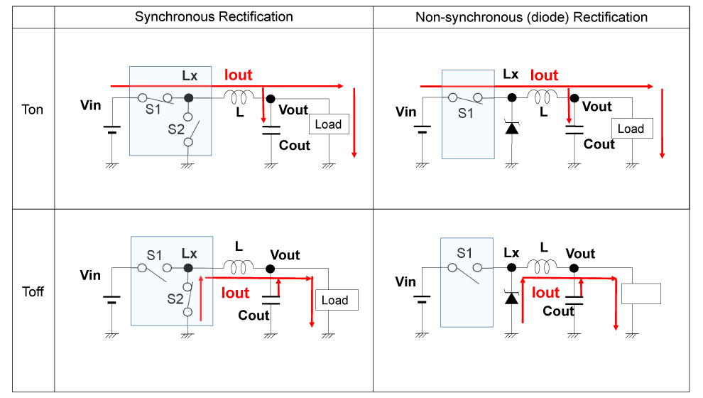
Figure 1. Configurations of Synchronous and Nonsynchronous (diode) Rectification in buck DC/DC converters
Both synchronous and nonsynchronous rectification have the same configuration of the high-side SW, S1, which turns on during the Ton period.
In synchronous rectification, the low-side SW, S2, is controlled to turn on as soon as the high-side SW, S1, turns OFF after the Ton period ends. The inductor tries to continue to flow the current, therefore, the inductor current is supplied from the GND through the low-side SW.
On the other hand, in nonsynchronous (diode) rectification, during the period when the high-side SW is on, the voltage of the Lx node becomes Vin, and the diode is not conductive because of the reverse biased voltage. Even if the high-side SW turns off, the inductor continues to flow the current, therefore, the energy of Lx node in Figure 1 is continuously discharged to the output. Because of the drastic drop of the Lx node voltage to being lower than the GND level, the forward current begins to flow through the diode, and the inductor current is supplied from the GND.
Comparison of Operation at Light Loads
As shown in Figures 2(1) and 2(2), when the load current is more than 1/2 of the inductor ripple current, both synchronous and nonsynchronous (diode) rectification are equal in operation. However, if the load current is less than 1/2 of the ripple current, the operation is different.
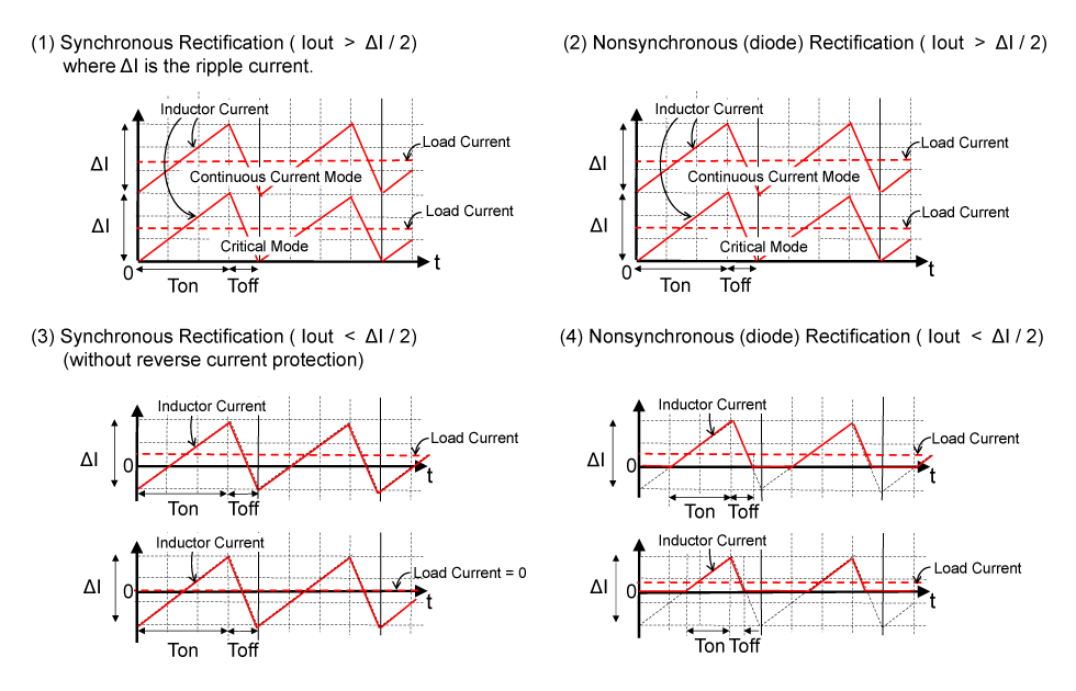
Figure 2. Comparison of Inductor Current between Synchronous and Nonsynchronous (diode) Rectification in PWM Control
In the synchronous rectifier without reverse current protection circuit, as shown in Figure 2(3), even if the load current becomes less than 1/2 of the ripple current, the operation does not change while maintaining the time ratio of Ton and Toff. Therefore, the inductor current becomes negative if the load current becomes less than half of the ripple current. In other words, the current from Vout to GND continues to increase, and the inductor stores energy because of this reverse current. Even if the low-side SW turns off and the high-side SW turns on, the inductor tries to continuously flow the reverse current. Therefore, the current flows in reverse from Vout to Vin through the inductor until the energy stored by the current flowing from Vout to GND becomes zero. This is shown in Figure 3.
Consider the case of zero load current as shown in Figure 3. In this case, after all the current supplied from Vin and GND is stored in the output capacitor Cout, the same intensity of current flows in reverse from Cout to GND and Vin. In other words, all current supplied by Vin is returned to Vin, therefore, it shows that there is no loss of energy in an ideal circuit even if the inductor current flows in reverse.
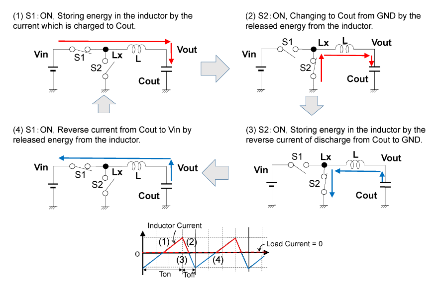
Figure 3. Reverse Current of Synchronous Buck DC/DC Converters at Zero Load Current
Because synchronous rectification without reverse current protection allows reverse current to operate continuously over the entire range of load current, the output voltage, Vout, is expressed as:
Vout = Vin × Ton / (Ton + Toff).
On the other hand, in nonsynchronous (diode) rectification, as shown in Figure 2(4), because the diode does not allow a flow of the inductor current in reverse, both the high-side SW, S1, and the diode turn off, and there is a period when the current is zero. This is called discontinuous conduction mode (DCM). In the discontinuous conduction mode, time ratio control is not possible.
Comparison of Efficiency between Actual Synchronous and Nonsynchronous Rectification
Because I explained so far based on ideal SWs and ideal diodes, both have 100% efficiency. From here, I would like to compare the efficiency of synchronous and nonsynchronous rectification with actual SWs and diodes.
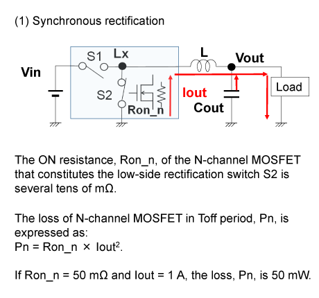
Figure 4. Comparison of Loss in Toff Period between Synchronous and Nonsynchronous Buck DC/DC Converters
As shown in Figure 4(1), MOSFETs are generally used for SWs. The on-resistance of MOSFET, which means resistance of MOSFET in conductive state, used in DC/DC converters is generally less than few tens or few hundreds of mΩ. (The larger the MOSFET size is, the lower the on-resistance is.)
On the other hand, as shown in Figure 4(2), a Schottky barrier diode, which has relatively small forward voltage Vf, is used in the nonsynchronous converter. The Vf voltage of the Schottky barrier diode is generally in the range of 0.3V to 0.5V.
Let us calculate and compare the losses in the case of 1A load current, where the on-resistance of the low-side SW, S2, for synchronous rectification is 50mΩ, and the Vf of the nonsynchronous rectification diode, D1, is 0.5V, respectively. The losses of synchronous and nonsynchronous rectification are equivalent at Ton, so let's compare the losses at Toff.
[Efficiency Loss Comparison at Toff]
-
- In the Case of Synchronous Rectification
Because a current of 1 A flows through the on-resistance of 50 mΩ, the power dissipation across the SW, W, is expressed as:
- W = I2 × R.
Therefore, the power loss of Toff period, W, is:
- W = 50 mW.
-
- In the Case of Nonsynchronous Rectification
The power dissipation across the diode, W, is expressed as:
- W = I × Vf.
Because the Vf of the diode is 0.5V and the flow of the current is 1 A, the power dissipation during Toff period is expressed as:
- W = 500 mW.
In these cases, the loss during the Toff period of nonsynchronous (diode) rectification is an order of magnitude larger than that of synchronous rectification.
The nonsynchronous (diode) rectification method has the advantage of simplifying the design of control circuits in DC/DC converters, because it only requires control of SW S1 to store energy in the inductor. Therefore, it has been widely used. However, the voltage supplied by DC/DC converters is becoming lower as LSIs such as CPUs become finer and more integrated. This means that Toff period becomes longer when the input voltage to the DC/DC converter is assumed to be constant. In other words, the output current flows through the rectification diode for a longer period, so the loss due to the Vf voltage of the rectification diode can no longer be ignored, as shown in the previous calculation. For this reason, synchronous DC/DC converters have become the mainstream.
Improvement in Efficiency of Synchronous Rectification at Light Load by Adding a Reverse Current Protection Function
In synchronous rectification, when the load current is smaller than half of the ripple current, the inductor current flows in reverse. This reverse current flowing through the resistive component of the high-side and low-side MOSFET SW causes loss. This is one of the factors that reduces the efficiency of synchronous rectification at light loads. A DC/DC converter with added reverse current protection function, which turns off the low-side MOSFET when detecting reverse current, reduces this loss.
If the reverse current of low-side is prevented, storing energy in the inductor by reverse current does not occur, and thus reverse current to the high-side to release the stored energy does not occur either. To prevent the reverse current, turn-off control is only required for low-side SW.
By adding a reverse current protection function, the operation of synchronous DC/DC converters at light load is equivalent to that of nonsynchronous (diode) DC/DC converters.
Note: PWM Control with or without Reverse Current Protection
The operation of synchronous DC/DC converters with PWM control differs depending on “with” and “without” reverse current protection. In general, the case of “with” reverse current protection which operates in a similar way to nonsynchronous (diode) rectification is designated as "normal PWM." The case of “without” reverse current protection is designated as "forced PWM."
High-frequency Noise Generated by Discontinuous Conduction Mode due to Reverse Current Protection
In synchronous DC/DC converters without reverse current protection (Forced PWM), the inductor current flows in reverse when the load current falls below the average value of the inductor ripple current (= half of the ripple current) at light loads. The inductor current flows continuously and the PWM operation, which regulates the output voltage by the time ratio, can be maintained as in the case of heavy load. The inductor current continuously flows in this case and this operation is called the continuous conduction mode (CCM). Figure 5(1) shows an image of the operation waveform of the Lx node and inductor current in this case.
Figure 5. Comparison of Operation Waveform between Synchronous Rectification with and without Reverse Current Protection
On the other hand, when the reverse current protection function is activated, the low-side SW turns off at the moment when the inductor current begins to flow in reverse. As a result, the period of zero inductor current continues. This operation is called discontinuous conduction mode (DCM). When the supply path of inductor current at the Lx node is interrupted, LC oscillation (ringing) occurs at the Lx node due to energy stored in the inductor and parasitic capacitance as shown in Figure 5(2). Thus, this results in high-frequency noise.
Efficiency Loss of DC/DC Converters
I mentioned briefly about loss of synchronous rectification and nonsynchronous (diode) rectification, here, I also explain the factors of loss in general DC/DC converters.
The efficiency of ideal DC/DC converters is 100%, but actual DC/DC converters have several loss factors that make efficiency worse. Losses can be roughly classified into two types: DC loss due to the load current Iout, flowing through the resistive component of the circuit, and AC loss due to the switching operation of DC/DC converters.
I will explain the main loss factors in synchronous buck DC/DC converters here. So far, we have shown DC/DC converters using only simple SWs' diagram. Now, please look at Figure 6-1 which shows the real circuit elements to explain the loss factors. The high-side SW is replaced by a P-channel MOSFET and the low-side SW by an N-channel MOSFET, and a SW control circuit is added.
Figure 6-1. Circuit Diagram of Synchronous Buck DC/DC Converters to explain Main Loss Factors
(1) DC Loss
There is a loss caused by the load current Iout, flowing through the resistive component of the SWs and the direct current resistive (DCR) components of the inductor during the Ton and Toff periods. There is power loss consumed by the control circuit. These losses fall into this category. Figure 6-2 shows the main DC loss factors.
-
1. Loss due to On-resistance of Pch/Nch MOSFET SW
The on-resistance, which means the resistance component during conduction state, of the MOSFET as a SW is few tens or few hundreds of mΩ. The loss during the Ton period is occurred due to on-resistance, Ron_p, and Iout of P-channel MOSFET SW, and the loss during the Toff period is occurred due to on-resistance and Iout of N-channel MOSFET SW. The loss during the Ton and Toff periods are expressed as:
- Pon = Ron_p × Iout2 × Ton / T, and
- Poff = Ron_n × Iout2 × Toff / T,
- where T is the period of PWM operation.
2. Loss due to Direct Current Resistance (DCR) of Inductors
Because the load current, Iout, flows continuously through DCR of the inductor in continuous conduction mode of PWM operation, the loss, Pdcr, is expressed as:
- Pdcr = Rdcr × Iout2.
3. Loss due to Power Consumed by the Control Circuit
In the PWM control method, because the SW control circuit is continuously operating, the loss, Picc, is generated due to the current consumption, Icc, of the SW control circuit.
- Picc = Icc × Vin.
Because this loss is constant regardless of Iout, it is one of the factors that makes efficiency worse at light load.
-
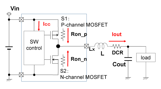
Figure 6-2. Loss Factors of Synchronous Buck DC/DC Converters (DC loss)
(2) AC Loss
This loss occurs during SW switching. Therefore, it is also called switching loss. Figure 6-3 illustrates the main AC loss factors.
-
1. Loss due to Charge/Discharge of Gate Capacitance of P-channel / N-channel MOSFET SW
Turning on and off of MOSFET SW is controlled by changing the gate voltage between 0V and Vin level through charging and discharging the gate capacitance of the MOSFET. In one cycle of PWM operation, the electrical charge which is charged and discharged at the gate capacitances of the MOSFET SW, Cg_p and Cg_n, are expressed as:
- Q = (Cg_p + Cg_n) × Vin.
Because the total amount of charge consumed per second corresponds to the consumption current, the power consumption (loss), Pgate, due to charging and discharging of gate capacitance is expressed as:
- Pgate = (Cg_p + Cg_n) × Vin2 × Fsw,
- where Fsw is the oscillation frequency for PWM operation.
*In PWM control, this loss is constant regardless of Iout, therefore, this is one of the factors contributing to efficiency loss at light load. This loss may be included in the DC loss due to power consumption of the SW control circuit.
2. Loss due to ON/OFF Transition Time, Tr/Tf, of MOSFET SW
- Loss for Tr period:
At the instant when the high-side P-channel MOSFET SW turns on, the voltage of Lx node is 0V. Since the Iout current flows through the P-channel MOSFET SW under Vin voltage applied across both ends of it, power loss occurs. However, after Tr time, the voltage of Lx node becomes Vin level (on-resistance of P-channel MOSFET is negligible), therefore, there is no loss. Thus, the loss for one Tr period can be calculated using the average of the voltages at both ends of P-channel MOSFET during the Tr period.
- Loss for Tf period:
It can be calculated using the same idea as in the case of Tr. Therefore, the loss for the Tr and Tf periods, Ptrtf, is expressed as:
- Ptrtf = 1/2 × (Tr + Tf) × Vin × Iout × Fsw.
-
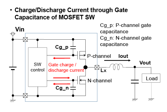
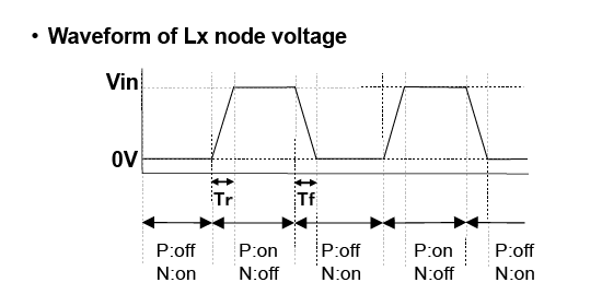
Figure 6-3. Loss Factors of Synchronous Buck DC/DC Converters (AC loss)
DC/DC Converters' Variation
Specifically, there is a synchronous PWM method with reverse current protection function to reduce DC loss in comparison with a nonsynchronous (diode) rectification method. There is also a synchronous rectification PWM method without reverse current protection for improvement of noise. In addition, the VFM(PFM) method has been added to the lineup to further improve efficiency at light load.
- Nonsynchronous (diode) rectification → Synchronous PWM method with reverse current protection (improvement for DC loss)
- Synchronous PWM method with reverse current protection → Synchronous PWM method without reverse current protection (improvement for noise)
- Synchronous PWM method with reverse current protection → Synchronous VFM(PFM) method (improvement for AC loss)
In the previous time, I explained that in the VFM(PFM) control method, which is a control method to improve efficiency at light load, the noise frequency spreads to lower frequency because the switching cycle becomes longer as the load current decreases. Furthermore, because the VFM (PFM) control method basically operates in discontinuous conduction mode, this method generates high-frequency noise due to ringing, immediately after current interruption.
For these reasons, different control methods for synchronous DC/DC converters are available to suit different applications, such as those that prioritize efficiency or noise suppression.
- Applications where efficiency is a top priority: synchronous DC/DC converters that can switch between VFM(PFM) method at light load and PWM with reverse current protection during the entire range of loads.
- Applications where noise suppression is important: synchronous DC/DC converters that allow reverse current.
* The former is called PWM/VFM(PFM) auto-switching, and the latter is called forced PWM.
Recently, a single product that can switch between the synchronous rectification PWM/VFM auto-switching method and the forced PWM method has been developed. The synchronous rectification PWM/VFM auto-switching method focuses on high efficiency, and the forced PWM method focuses on noise suppression by allowing reverse current flow and operating in continuous conduction mode over the entire range of load currents. Products with anti-ringing measures have also been developed to suppress high-frequency noise caused by discontinuous conduction mode.
Table 1 shows the characteristics of each of the rectification methods described above.
Table 1. Comparison of Synchronous and Nonsynchronous (diode) Rectification Method
| Synchronous rectification | Nonsynchronous (diode) rectification | ||
|---|---|---|---|
| without reverse current protection | with reverse current protection | ||
| Efficiency Loss for Toff period |
Good | Bad | |
| On-resistance of rectification SW: Small | Loss due to rectification diode VF: 0.3-0.5V: Large | ||
| Noise | Good | Bad | Bad |
| Continuous conduction mode operation only | high frequency noise due to LC oscillation in discontinuous conduction mode | high frequency noise due to LC oscillation in discontinuous conduction mode | |
| Design | simple | complicated | simple |
| External components | Cin, Cout | Cin, Cout, and Schottky Barrier Diode (SBD) | |
Conclusion
I would like to continue one more lesson. Next time, I will summarize what we have learned so far and that will be the last lesson about DC/DC converters.
Thank you for reading.
Power Management IC Basics
- Vol. 1
What Are Power Management ICs? - Vol. 2
What Is a Linear Regulator (LDO Regulator)? Part 1 - Vol. 3
What Is a Linear Regulator (LDO Regulator)? Part 2 - Vol. 4
What Is a Linear Regulator (LDO Regulator)? Part 3 - Vol. 5
What Is a DC/DC Converter? Part 1 - Vol. 6
What Is a DC/DC Converter? Part 2 - Vol. 7
What Is a DC/DC Converter? Part 3 - Vol. 8
What Is a DC/DC Converter? Part 4 - Vol. 9
What Is a DC/DC Converter? Part 5 NEW
Author profile

Lecturer S (Nisshinbo Micro Devices Inc.)
For a long time since he joined the company, he has been involved in various analog and digital designs such as gate arrays, microcomputers, memories, and power management ICs. After that, he also mastered the test technology of compound power supply ICs and became a specialist in design, testing and education on his specialty. His easy-to-understand explanations and polite guidance from the listener's perspective are well received by new engineers who join our company every year. His achievements are highly commended, and now he is working as a senior engineer in training younger generations and as a consultant for new technologies.
FAQ: DC/DC Switching Regulators
- What is a soft-start function?
- What is the circuit configuration and pin treatment when not using the R1283 boost circuit?
- The data sheet for the FB pin of the NJM2369 says that the source current is 40 to 200µA, but does this pin have a built-in pull-up resistor?
- What is an over-current protection (OCP) for DC/DC converters?
- What is externally programmable maximum duty cycle?