


Power Management IC Basics Vol. 2:
What Is a Linear Regulator (LDO Regulator)?
Negative feedback circuit Dropout voltage
Introduction
In the previous volume of this series, we briefly explained to you where and how power management ICs are used in the world. In this page, we will explain one kind of voltage regulator called linear regulator.
Do you remember that there are two types of voltage regulators: the linear type and the switching type?
Linear-type regulators can be further separated into two types: the series type, which inserts a transistor as a variable resistor in series between the input and the load*1, and the shunt type, which inserts a transistor in parallel with the load. In this lecture, we will focus solely on the series-type linear regulator, as this type is more commonly used than the shunt type whose usage is quite limited. Now let’s get started.
Linear Regulators
The simplest regulators are called 3-pin regulators, which output a stable fixed voltage just by inserting an input capacitor (CIN) between the VIN and the GND pins, and an output capacitor (COUT) between the VOUT and the GND pins.
Then, how can those regulators output a stable fixed voltage?
We will describe what components linear regulators contain and how they output a fixed voltage.
Figure 1 below shows a brief illustration of a circuit structure of a linear regulator.
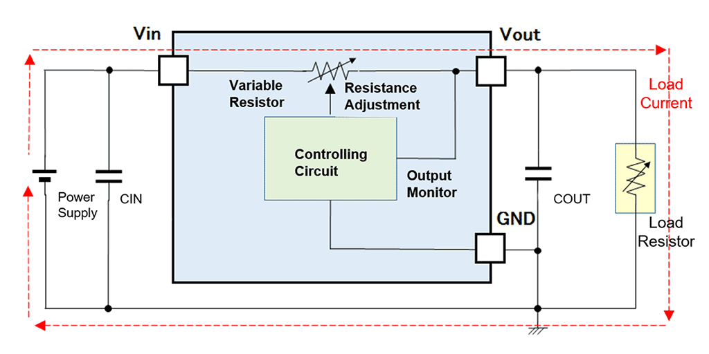
The controlling circuit monitors Vout and adjusts resistance value of the variable resistor so that the linear regulator can generate a fixed output voltage.
Figure 1. Simplified Internal Structure of Linear Regulator
The figure illustrates that the controlling circuit supervises the output voltage and regulates the resistance value of the variable resistor so that the IC can output the set fixed voltage. For instance, if the input voltage (VIN) is fixed, a linear regulator can maintain a stable output voltage by keeping the ratio between the variable resistance value and the load resistance value fixed according to the changing rate of the load resistance value. The input voltage is divided by the two resistors, so linear regulators generate a lower output voltage than their input voltage. The difference between the higher input voltage and lower output voltage will generate heat which is called waste heat. The current flowing inside the load resistor goes on to flow to the variable resistor, where the electricity is consumed with some heat generated.
Figure 2 illustrates these relationships. For example, in the case of load current at 100 mA, a 5 V input and 2 V output regulator consumes 0.3 W of 0.5 W input electric power inside as heat.
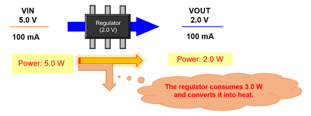
The linear regulator consumes some of the input power and converts it into heat in order to generate a fixed output voltage.
Figure 2. Operation Image of Linear Regulator
Circuit Structure of Linear Regulator
Linear regulators have four fundamental components: an output driver transistor, a reference voltage unit, a feedback resistor, and an error amplifier. Figure 3 shows a basic structure of a typical linear regulator.
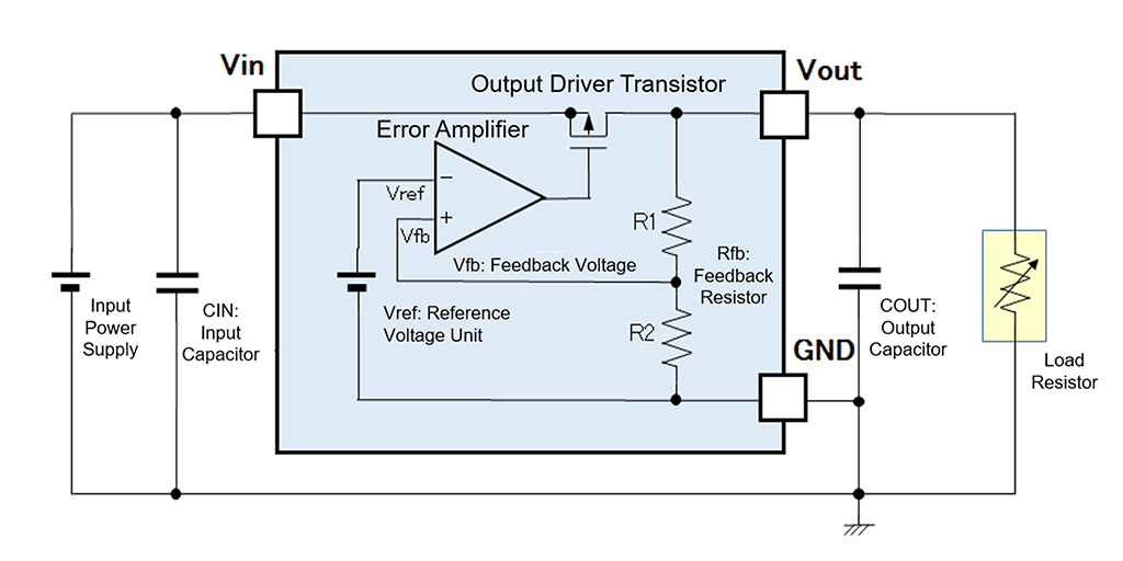
Figure 3. Basic Structure of Linear Regulator
The roles of each components are as follows:
1. Output Driver Transistor
Figure 3 is an example of a linear regulator constructed with a MOS transistor. This transistor is equivalent to the variable resistor shown in Figure 1.
As is shown in Figure 2, where the load and input currents are equal at 100 mA, the VIN pin supplies all the current flowing through the driver transistor and the VOUT pin to the load. Linear regulators maintain a fixed output voltage by regulating the resistance of the driver transistor with a controlling circuit (shown in Figure 1) composed of a feedback resistor, a reference voltage unit, and an error amplifier.
2. Feedback Resistor
A feedback resistor (RFB) is named after its role of dividing the output voltage with two resistors (R1 and R2) and returning the divided voltage to an error amplifier. The divided voltage is called a feedback voltage (VFB). The subscript "FB" represents FeedBack. A feedback resistor takes the role of deciding a fixed output voltage level of the linear regulator, and the output voltage level is determined by the resistance ratio of R1 and R2.
The output voltage range is specified by products, and within the specified range, the output voltage can be generated by adjusting with laser trimming the resistance ratio of R1 and R2 of each wafer die on the entire wafer fabricated in a manufacturing process.
Also, some of linear regulators have a VFB pin to connect an optimal external feedback resistor, which enables users to flexibly set the output voltage.
3. Reference Voltage Unit
There are some methods to construct a reference voltage unit, and most of them provide an output voltage level of around 1 V.
A conventional method used for a reference voltage unit is called a band gap reference (BGR). Although this method has good characteristics, its supply current and circuit structure tend to be larger, for it utilizes the voltage between the base and the emitter of a bipolar transistor. 1.25V is a commonly used output voltage level for a BGR.
Instead of BGRs, more electronic equipment utilizes a CMOS-based voltage reference unit. A CMOS-based reference unit uses the difference between the threshold voltage of two MOS transistors as a reference voltage. It features a small circuit size and an extremely low supply current. Its output voltage level is from about 0.6 to 1.0 V. It is depicted in Figure 3 with a battery symbol.
Reference voltage units can maintain a certain voltage level despite the fluctuations in the input voltage or the changes in the ambient temperature. Thanks to the reference voltage unit keeping a certain level of a reference voltage, linear regulators can output a fixed voltage.
4. Error Amplifier
An error amplifier is a kind of operational amplifier that amplifies the voltage difference between two input terminals (positive and negative) and outputs the amplified voltage.
Inside a linear regulator, the positive terminal receives the feedback voltage, and the negative terminal receives the reference voltage. The error between the two voltages is amplified inside the operational amplifier, and the amplified voltage is output to the variable resistor. This is why the component is called error amplifier.
In summary, linear regulators include a negative feedback circuit which consists of the four components mentioned above and make their output voltage constant by negative feedback control*2. Negative feedback control compares the feedback voltage with the reference voltage and regulates the resistance of the output driver transistor so that the difference becomes zero.
Accordingly, in a normal state, the VREF and VFB are kept equal.
The relationship can be represented by the following equation:
VFB = VREF ... [1]
VFB = VOUT × R2 / (R1 + R2) ... [2]
Incorporate equation [1] for VFB in equation [2]:
VREF = VOUT × R2 / (R1 + R2) ... [3]
∴ VOUT = VREF × (R1 + R2) / R2
This equation does not consider the input voltage nor the load current (load resistance). It represents that the output voltage is determined simply by the reference voltage and the resistance ratio of the feedback voltage at a normal state.
According to this equation, too, it can be said that the voltage reference (VREF) is the key component which determines the characteristics of a linear regulator.
Also, the variability of the resistance values does not matter, because the output voltage is determined by the resistance ratio of R1 and R2. As resistors are fabricated and located in a considerably small area inside a semiconductor chip, the resistance ratio becomes highly accurate.
Then, how do linear regulators control the resistance of the driver transistor to output a stable voltage, even when the load current (load resistance) or the input voltage fluctuates?
The mechanism can be explained from the perspectives of the output driver On-resistance and the output load resistance ratio.
Let us take an example of a linear regulator whose specifications are as follows: the reference voltage of 1 V, equal resistance between R1 and R2, and the output voltage of 2 V. In the case of 5 V input and the load current of 200 Ω, the regulator controls the resistance of its output driver to 300 Ω. In other words, the regulator controls the ratio between the driver On-resistance and the load resistance so as to divide the output voltage by 3:2.
- The Case of Load Current Fluctuation
How about the case where the load resistance changes from 200 Ω to 20 Ω? The regulator controls its output driver resistance from 300 Ω to 30 Ω in order to keep the resistance ratio at 3:2 and to output a preset 2 V. - The Case of Input Voltage Fluctuation
Then, how about the case where the input voltage changes from 5 V to 4 V? The output voltage would become 1.6 V if the initial resistance ratio were kept. To keep a stable 2 V, the regulator controls not only the output driver resistance from 300 Ω to 200 Ω but also the resistance ratio from 3:2 to 1:1.
As is shown above, linear regulators can supply a stable output voltage even under variations in the load current or the input voltage. The level of output stability is defined as line regulation, and load regulation. Below is a detailed explanation.
Line Regulation (ΔVOUT/ΔVIN): Max. 0.2%/V (VSET + 0.5 V < VIN < 5 V)
Load Regulation (ΔVOUT/ΔIOUT): ±40 mV (1.5 V ≤ IOUT ≤ 100 mA)
Operation of Linear Regulators
In accordance with Figure 4, let us check the flow of the internal operation of a linear regulator when its output load resistance changes.
Linear Regulator's Operation against Load Fluctuations
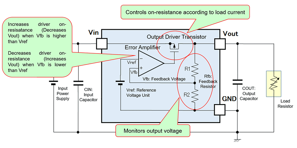
Figure 4. Linear Regulator’s Operation at Load Current Fluctuation
As the load resistance decreases and the load current increases, the output voltage and the feedback voltage decrease at the same time. The output voltage from the error amplifier also decreases as the feedback voltage becomes lower than the reference voltage, which as a result decreases the driver On-resistance. The decrease of the output driver On-resistance according to the increase of the load current consequently leads the output voltage to restore its set value. By the output voltage returning to the set value, the feedback voltage coincides with the reference voltage.
Reversely, the decrease of the load current increases the output voltage of the error amplifier and the driver On-resistance, because it raises the output and feedback voltages. The rise of the driver On-resistance in accordance with the decrease of the load current makes the output voltage return to its set value.
LDO Regulators
By the way, some of linear regulators are classified as LDO regulators. LDO is an abbreviation for Low DropOut. What does ‘low dropout’ mean?
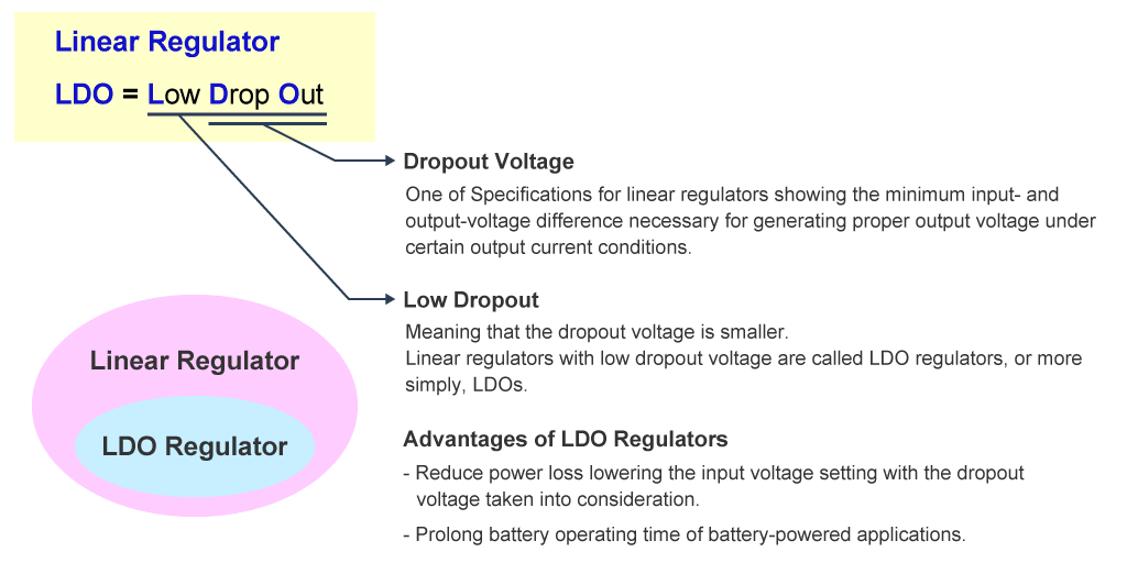
Figure 5. What does ‘LDO’ mean?
A linear regulator has a specification defined as dropout voltage (VDIF). Dropout voltage refers to the minimum difference between input and output voltages necessary for linear regulators to generate a set output voltage within a permissible range*3. Linear regulators will fail to maintain the set output voltage and the output voltage will drop when the difference between the input and output voltages becomes smaller than the dropout voltage.
Let us take an example of a linear regulator receiving electricity from a battery. If the input voltage to a linear regulator exceeds the sum of the set output voltage and the dropout voltage, the regulator can provide stable output voltage. Accordingly, the lower the dropout voltage of the linear regulator, the longer the battery operating time becomes.
Then, how about a linear regulator whose source voltage is supplied from a DC/DC converter? The DC/DC converter is being set to output a voltage a little higher than the sum of the output voltage and dropout voltage of the linear regulator. In this case, compared to using a linear regulator with dropout voltage of 0.4 V, a regulator with dropout voltage of 0.2 V can halve power loss. In short, using a regulator with low dropout voltage can reduce power loss.
Remember that replacing the linear regulator with one whose dropout voltage is 0.2 V cannot reduce power loss without adjusting the set output voltage of the DC/DC converter.
This benefit differentiates linear regulators with low dropout voltage regulators or simply referred to as LDO regulators. However, there is no standard definition for LDOs, so it differs from company to company. Therefore, in many cases, LDO is used as a brief expression for any kind of linear regulators.
Dropout Voltage and Output Current
Case of 3.0 V Output LDO with Dropout Voltage of Maximum 0.23 V (Iout = 150 mA)
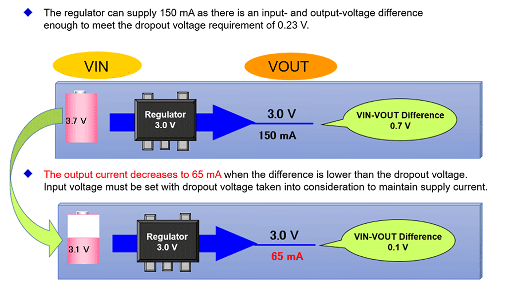
Figure 6. Image of Dropout Voltage and Output Current
Dropout voltage is determined under a specific output condition. For example, figure 6 shows a dropout voltage with output current at 150 mA. As mentioned above, a driver transistor is a kind of variable resistor. Then, let's think about the relation between dropout voltage and output current by Ohm's law, regarding a driver as a resistor.
In this example, the minimum value of dropout voltage is 0.23 V, and the output current condition at that moment is 0.15A. By Ohm's law, the driver resistance is calculated as follows:
R = V/I = 0.23/0.15 = 1.53 Ω
This calculation suggests the minimum driver resistance of the LDO regulator.
Next, based on this resistance, let's calculate the permissible output current in the case of the input-output voltage difference of 0.1 V.
I = V/R = 0.1/1.53 = 0.0652 A
The calculation result suggests that in order to maintain 3.0 V output at 3.1 V input, the output current of this LDO regulator must be below 65 mA. This also means that if this LDO regulator outputs 150 mA at 3.1 V input, the output voltage will be 2.87 V. This will result in the output voltage to be lower than the input voltage by 0.23 V and the set output voltage by 0.13 V.
Figure 7 illustrates the relationship between input and output voltage with a graph.
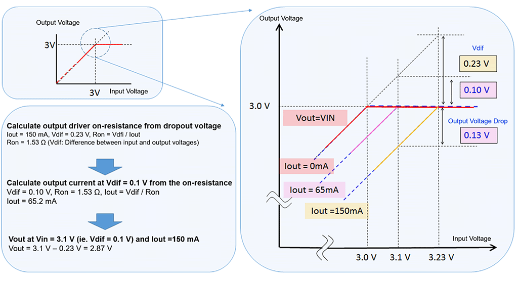
Figure 7. Relationship between Dropout Voltage and Output Current
According to the calculation above, connecting a driver transistor in parallel can make this LDO regulator output 150 mA at 3.1 V, as it can reduce in half the driver's on-resistance and double the output current.
However, as Picture 8, a photo of the LDO regulator’s circuit shows, most of the chip area is occupied by a driver.
To double the output current or to halve the dropout voltage will require reducing the resistance. This can be accomplished by constructing two driver transistors in parallel in this limited space.
Constructing two drivers in parallel means doubling the driver area and chip area which leads to an increase in the price. There needs to be a balance between regulator specifications and price.
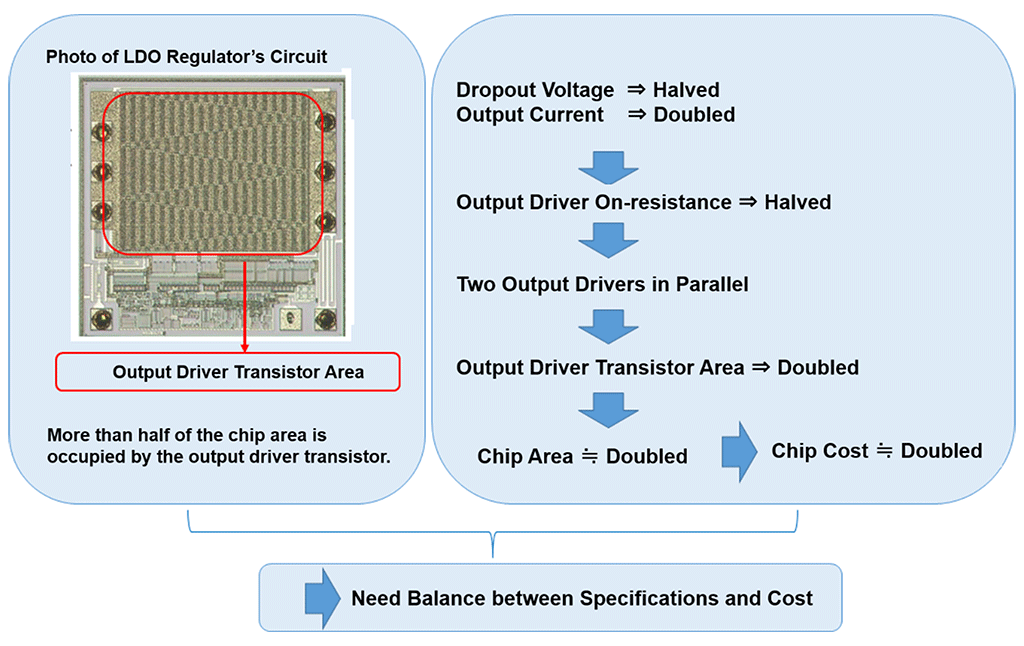
Figure 8. Chip Photo of General LDO Regulator
Conclusion
In this lecture, we have explained the mechanism of how a linear regulator keeps a stable output voltage regardless of input voltage or load current fluctuations.
In summary, a linear regulator monitors the output voltage and keeps stable output voltage with a negative feedback circuit which adjusts the internal driver's on-resistance. This mechanism enables a linear regulator to output a stable voltage even when input-voltage or load-current fluctuations cause a gap between the output voltage and the set voltage.
Also, we have introduced some specifications which show the output stability of a linear regulator, such as input regulation, load regulation, and dropout voltage which is necessary to keep a stable output voltage.
These specifications are time-independent.
Next, we are going to explain time-dependent specifications, power dissipation limitation to keep linear regulators operation stable, roles of input and output capacitors, and so on.
Thank you for reading!
Notes
- *1 A load device is one that operates with a stable voltage supplied from a power management IC and power source. Here, we treat one or more load devices as a resistor collectively, and a current flowing to the load is called a load current.
- *2Taking an example of a car moving on a rising slope at a speed of 100 kilometer an hour will help understand negative feedback control. To keep that speed, the driver steps on the accelerator to raise the engine power while watching the speedometer. If the speed exceeds 100 km/h, the driver will decrease it by easing up on the accelerator to reduce the engine power. Also, the driver will increase the speed if the speed falls below 100 km/h. This is also a kind of negative feedback control, as the driver controls the engine power in opposite directions according to the speed s/he monitors.
Let's go back to the original topic. Replacing the following words will enable you to grasp negative feedback control used in a linear regulator.
- engine power = output driver's on-resistance
- 100 km/h = reference voltage
- speedometer = feedback voltage or output voltage
- driver = error amplifier
- incline of the rising slope = amount of load current
- *3 To differentiate dropout voltage as a specification of an LDO regulator from the literary meaning of the difference between the input and output voltages of an IC, the term 'dropout voltage' is used in the description.
Power Management IC Basics
- Vol. 1
What Are Power Management ICs? - Vol. 2
What Is a Linear Regulator (LDO Regulator)? Part 1 - Vol. 3
What Is a Linear Regulator (LDO Regulator)? Part 2 - Vol. 4
What Is a Linear Regulator (LDO Regulator)? Part 3 - Vol. 5
What Is a DC/DC Converter? Part 1 - Vol. 6
What Is a DC/DC Converter? Part 2 - Vol. 7
What Is a DC/DC Converter? Part 3 - Vol. 8
What Is a DC/DC Converter? Part 4 - Vol. 9
What Is a DC/DC Converter? Part 5 NEW
Author profile

Lecturer S (Nisshinbo Micro Devices Inc.)
For a long time since he joined the company, he has been involved in various analog and digital designs such as gate arrays, microcomputers, memories, and power management ICs. After that, he also mastered the test technology of compound power supply ICs and became a specialist in design, testing and education on his specialty. His easy-to-understand explanations and polite guidance from the listener's perspective are well received by new engineers who join our company every year. His achievements are highly commended, and now he is working as a senior engineer in training younger generations and as a consultant for new technologies.
FAQ: LDO Linear Regulators
- What is a soft-start function?
- Does the Reverse Current Protection Function of the R1191 work regardless of the CE status (H/L)?
- Regarding the output current of the NJM2871A, the maximum value is stated to be 150mA, but is there a minimum value?
- What is the input to CE pin when putting this series into standby state?
- How much is the value of CE pin's pull-down resistance of RP122?