


Power Management IC Basics Vol. 4:
What Is a Linear Regulator (LDO Regulator)? Part 3
Introduction
In the previous volume, we briefly mentioned power dissipation, which we were going to talk about when explaining DC/DC converters (switching regulators). However, as power dissipation is highly important to use linear regulators, we will talk about efficiency and power dissipation of linear regulators.
Efficiency of Linear Regulator
Efficiency of Power Management IC
First, let me provide an overview of efficiency of a power management IC. The role of a power management IC is to supply stable voltage and power necessary for the load device to operate. Ideally, a power management IC should be able to provide all the electricity from an input power supply to its load device. However, it also requires some electricity to generate and supply a stable voltage to the load. Therefore, an "efficient power management IC" means the one which requires low electricity to generate a fixed voltage.
Efficiency is expressed by the proportion between the power the load device consumes and the power the input power supply provides for the power management IC.
Efficiency (%) = Output Power (W) / Input Power (W)
Efficiency is one of the important indicators suggesting performance of a power management IC.
Efficiency of Linear Regulator
Figure 1 is a block diagram of a linear regulator which shows currents flowing through each block, power consumption at each block, and efficiency calculated from the power consumption.
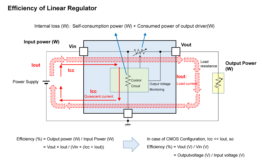
Figure 1. Efficiency of Linear Regulator
The current flowing through the linear regulator is the sum of the quiescent current Icc and the output current Iout. Therefore, the input power is calculated by the formula below:
Input Power (W) = Vin × (Icc + Iout).
The power consumed inside the linear regulator (internal loss) consists of the self-consumption power which controlling blocks consume (Vin × Icc) and the power which the output driver consumes.
Therefore, internal loss can be expressed by the formula below:
Internal Loss (W) = Vin × Icc + (Vin – Vout) × Iout
Vin: Input Voltage
Vout: Output voltage
Iout: Output Current
Icc: Quiescent Current
Also, output power (W) is calculated by the following formula:
Output Power (W) = Vout × Iout
As is mentioned above, efficiency (%) can be calculated by dividing output power (W) by input power (W), and based on the formulas mentioned, the efficiency formula can be rewritten as shown below:
Efficiency (%) = (Vout × Iout) / ((Vin × (Icc + Iout)).
A CMOS-based linear regulator consumes very small current internally, so if the quiescent current is ignored, the efficiency will be calculated by the following formula:
Efficiency (%) = (Vout × Iout) / (Vin × Iout).
Moreover, you can delete the common denominator and numerator Iout:
Efficiency (%) = Vout (V) / Vin (V).
This means that the efficiency of a linear regulator can be briefly calculated by dividing its output voltage by its input voltage.
As a linear regulator consumes electricity in the output driver transistor to generate a fixed output voltage, it is far from an ideal power supply from the point of view of efficiency.
*From efficiency perspective, DC/DC converters (switching regulators) tend to be superior to linear regulators. We are going to explain performance and features of DC/DC converters in comparison with those of linear regulators in the following volumes.
As you can see by these equations, an LDO with very low dropout voltage can accomplish the efficiency equal to or superior to a DC/DC converter if the application can accept a small input-output differential. For instance, when an LDO with 0.3 V dropout receives 3.3 V input and generates 3.0 V output, it can achieve an efficiency of 91%, which means it can be as efficient as a DC/DC converter.
On the other hand, the efficiency deteriorates as the input-output voltage differential becomes larger. The power that does not enhance efficiency during conversion is seen as a loss of power.
Internal Loss (Consumed Power) and Power Dissipation of Package
Power dissipation is the acceptable value of electrical power which is consumed inside an IC and converted into heat. I will offer further explanations below.
A linear regulator generates stable output voltage by consuming power in its built-in output driver transistor, and the power consumed there is all converted into heat. This heat generation increases the temperature of the linear regulator. The problem here is that a linear regulator has a limited thermal value beyond which it can malfunction, or even worse, be damaged.
"Power dissipation" thus represents the maximum acceptable value of internal loss, or power consumption, to avoid surpassing this thermal limitation.
Then, how is the power dissipation calculated?
Thermal Resistance
The power consumed inside a semiconductor chip, or internal loss, turns into heat and increases the chip temperature. However, the generated heat radiates through the package containing the semiconductor chip. Therefore, the chip temperature is determined at the equilibrium point between the amount of semiconductor-chip heat generation and the package's capability of heat radiation.
How much heat a semiconductor chip generates is determined by the amount of consumed power or internal loss. Also, heat radiation capability of a package is determined by the package type, the size, the board which the chip is mounted on, etc.
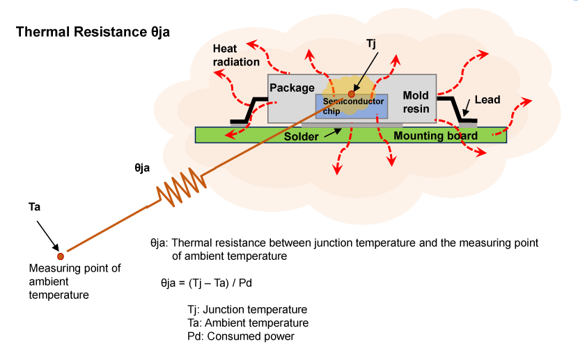
Figure 2. Thermal Resistance of a Package
Figure 2 shows how the heat generated by the chip radiates through all the paths it can use. In one example, when heat is generated by the surface of a chip mounted on a mold resin package, it radiates from the package surface via the mold resin. Or, in another example, the heat can be radiated from the lead frame to the leads, from the leads to the mounting board, and the mounting board to air.
A package with good heat radiation characteristics can suppress temperature increase of a chip for heat generated, as it can efficiently conduct heat from the heated portion to the surroundings. Conversely, a package with low heat conductance leads to temperature increase of a chip due to heat generation. This suggests that we can consider how difficult it is for heat to conduct due to temperature rise caused by a chip's heat generation. This is the concept of thermal resistance.
Thermal resistance can be calculated by the following formula:
θja = (Tj – Ta) / Pd
θja: Thermal resistance between junction and the measuring point of ambient temperature
Tj: Junction temperature
Ta: Ambient temperature
Pd: power consumption (internal loss)
Here, the subscripts "j" and "a" stand for "Junction" and "Ambient" respectively.
Generally, thermal resistance is expressed by the increased rate of the junction temperature to power consumption of a semiconductor chip, with the ambient temperature, the temperature at the point where the thermal increase of the package does not reach, considered as the basis.
By the way, the formula may be more understandable if you notice that it has the same structure as Ohm's Law:
R = V / I.
* Electrical Resistance and Thermal Resistance
- Electrical Resistance
A current flows from the higher electrical potential to the lower one. The amount of the current is proportional to the potential difference.
The constant of proportionality is called electrical resistance, which is calculated by the following formula:
Electrical Resistance = Potential (V) / Current (A)
- Thermal Resistance
Heat flows from the hotter point to the cooler point. The amount of the flow is proportional to the thermal differential. The constant of proportionality is called thermal resistance, which is calculated by the following formula:
Thermal Resistance = Thermal Differential (°C) / Thermal Flow (W)
Note: We assume here that the amount of heat flowing through thermal resistance is equal to the power consumption, as power consumption equals the amount of heat generated per second.
Electrical resistance refers to how difficult it is for a current to flow in a material, and thermal resistance refers to how difficult it is for heat to conduct through a material.
Maximum Junction Temperature Value (Tjmax)
Next, let us consider the junction temperature below which a semiconductor device can operate properly.
The maximum value of temperature under which a semiconductor product can stably work is determined as the maximum junction temperature (Tjmax). Normally, the value is 125°C or 150°C.
Junction temperature refers to the temperature at the PN junction, but it is considered and also used as the semiconductor chip’s temperature.
Power Dissipation of Package
- As mentioned above, each package has its own thermal resistance showing a heat radiation characteristic determined by the package itself and by the mounting board, which is represented by the formula:
θja = (Tj – Ta) / Pd.
Pd can be calculated by converting this formula into the one below:
Pd = (Tj – Ta) / θja
- Each semiconductor product has a maximum junction temperature (Tjmax) referring to the maximum thermal value below which a semiconductor device can operate properly.
From these two considerations, each package results in having a maximum value of power consumption or internal loss in order for a semiconductor chip mounted on the package never to surpass its maximum junction temperature (Tjmax).
This is what we call power dissipation of a package (Pd max). This can be calculated by the formula below which replaces Pd and Tj in the formula above with Pdmax and Tjmax:
Pdmax = (Tjmax - Ta) / θja
Pdmax: Power Dissipation
Tjamax: Maximum Junction Temperature
Ta: Ambient Temperature
θja: Thermal Resistance between Junction and Ambient Temperatures
To sum up the points mentioned thus far, power dissipation of a package refers to:
- the maximum value of power consumption or internal loss to let the device mounted in the package (here, a linear regulator as a power management IC) operate properly
- the maximum value of power consumption or internal loss below which a semiconductor product never generates more heat than its maximum junction temperature (Tjmax).
Power Dissipation Examples
Figures 3-1 and 3-2 show thermal resistance of a package mounted on a certain board and power dissipation of a semiconductor device with Tjmax of 125°C at an ambient temperature of 25°C. They also have a chart showing the relationship between power dissipation and ambient temperature.
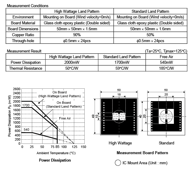
Figure 3-1. Power Dissipation Example 1
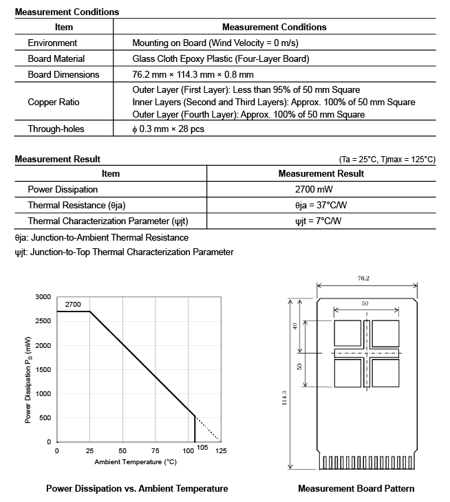
Figure 3-2. Power dissipation Example 2
In Figure 3-1, thermal resistances and power dissipations under the following three conditions are mentioned:
- no connection between the package and the board
- mounted on a two-layer board with a wiring ratio of 90%
- mounted on a two-layer board with a wiring ratio of 50%.
Figure 3-2 suggests thermal resistance and power dissipation when using a four-layer board with a higher wiring rate than those mentioned above.
These data tell us that thermal resistance and power dissipation of a package largely depend on the board the package is mounted on. Also, it seems that increasing the wiring ratio and the number of layers of a mounting board decreases thermal resistance and increases power dissipation.
What I would like to emphasize here is, as I have explained in Figures 3-1 and 3-2, that thermal resistance and power dissipation described in each package description are measurement results under certain conditions.
Thermal resistance and power dissipation will vary if the layout pattern and the copper ratio of a board changes. Therefore, the value in the datasheets or other technical documents should be considered only as a reference value.
The power dissipation of a package mounted on an actual board should be calculated by the thermal resistance estimated for the board. If you want to know the actual power dissipation of your board in detail, it will be helpful to ask IC manufacturers like us.
Power Dissipation and Input-output Voltage Differential
I have already shown in Paragraph "Efficiency of Linear Regulator" that the internal loss Pd of a regulator can be calculated by the following formula:
Pd = (Vin – Vout) × Iout + Vin × Icc
Instead of using the formula above, you can calculate the internal loss of a CMOS-based linear regulator, because its quiescent current is ignorable in a highly-large-current range within which power dissipation must be considered:
Pd = (Vin – Vout) × Iout
I will show the formula to calculate power dissipation again:
Pdmax = (Tjmax – Ta) / θja
You need to sufficiently consider the relationships between these formulas and select linear regulator products and packages.
Conclusion
In this volume, I explained power dissipation of linear regulators, for it is an important factor that warrants sufficient explanation.
In the next five consecutive volumes, I am going to talk about DC/DC converters.
Thank you for reading.
Power Management IC Basics
- Vol. 1
What Are Power Management ICs? - Vol. 2
What Is a Linear Regulator (LDO Regulator)? Part 1 - Vol. 3
What Is a Linear Regulator (LDO Regulator)? Part 2 - Vol. 4
What Is a Linear Regulator (LDO Regulator)? Part 3 - Vol. 5
What Is a DC/DC Converter? Part 1 - Vol. 6
What Is a DC/DC Converter? Part 2 - Vol. 7
What Is a DC/DC Converter? Part 3 - Vol. 8
What Is a DC/DC Converter? Part 4 - Vol. 9
What Is a DC/DC Converter? Part 5 NEW
Author profile

Lecturer S (Nisshinbo Micro Devices Inc.)
For a long time since he joined the company, he has been involved in various analog and digital designs such as gate arrays, microcomputers, memories, and power management ICs. After that, he also mastered the test technology of compound power supply ICs and became a specialist in design, testing and education on his specialty. His easy-to-understand explanations and polite guidance from the listener's perspective are well received by new engineers who join our company every year. His achievements are highly commended, and now he is working as a senior engineer in training younger generations and as a consultant for new technologies.
FAQ: LDO Linear Regulators
- What is a soft-start function?
- Does the Reverse Current Protection Function of the R1191 work regardless of the CE status (H/L)?
- Regarding the output current of the NJM2871A, the maximum value is stated to be 150mA, but is there a minimum value?
- What is the input to CE pin when putting this series into standby state?
- How much is the value of CE pin's pull-down resistance of RP122?