


Power Management IC Basics Vol. 3:
What Is a Linear Regulator (LDO Regulator)? Part 2
Introduction
In Volume 2, we have explained the general structure of linear regulators. Also, we have introduced some specifications including line regulation and load regulation which indicate the stability of output voltage, and dropout voltage which is necessary for a linear regulator to keep a stable output voltage. These specifications are time-independent.
In this volume, time-dependent specifications such as ripple rejection, input and load transient response, and relationships between these specifications and supply current will be explained. Also, I will talk about the importance of power dissipation of packages and protective functions for safe operation of linear regulators. Lastly, I will explain the roles of input and output capacitors.
Ripple Rejection
When converting a 50/60 Hz AC power derived from the outlet into a DC power with an AC adapter, the DC power contains hum noise, a small voltage fluctuation with a frequency of 50/60 Hz. Similarly, voltage variations with various frequencies occur in a power supply line depending on operations of devices connected to it. These small voltage fluctuations superimposed in the power supply line sometimes prevent power management ICs from supplying stable voltages. These small fluctuations repeat themselves in the power supply line, so they are called ripples, or ripple noise.
One of the main features of a linear regulator is that it reduces these ripple noise superimposed in the input voltage before the noise reaches the output side. This feature is represented as ripple rejection (RR). Sometimes this is also called power supply rejection ratio or power supply ripple rejection (PSRR).
Figure 1 is an image of this PSRR feature of a linear regulator, showing that ripple noise overlapping in the output voltage is almost removed in the output voltage.
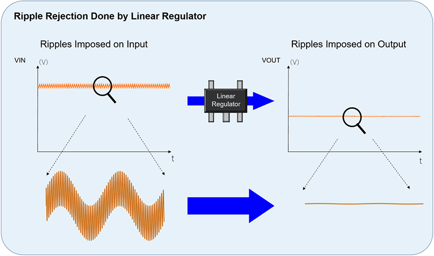
Figure 1. Ripple Rejection by Linear Regulator
Noise contains various frequency components, so ripple rejection should be evaluated for each sine wave of each frequency component. This is referred to as frequency characteristics of ripple rejection.
Ripple rejection has a wide numerical value range of 2 to 5 digits, so it is defined by the following formula using a logarithm for convenience. The measurement unit is dB.
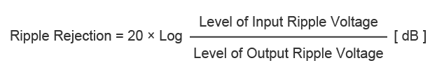
In general, electrical characteristics in datasheets show ripple rejection at the ripple frequency of 1 kHz. Regular linear regulators usually have a ripple rejection characteristic of around 40 to 60 dB, and those with high PSRR can achieve around 60 to 80 dB.
This means, for example, that a linear regulator with a ripple rejection characteristic of 60 dB at 1 kHz can output a voltage with 1/1000 ripple noise of the input voltage. More concretely, 1 kHz, 100 mVp-p ripple noise in the input voltage will be reduced to 0.1 mVp-p in the output voltage.
Figure 2 shows the frequency characteristic of the RP122 LDO regulator with industry-leading ripple rejection ratio. Ripple rejection tends to decrease as the frequency increases and varies depending on the load current and the gap between input and output voltage levels. You need to consult datasheets of each manufacturer according to your actual usage, as they contain graphs of ripple rejection under various conditions that vary the amount of load current or gap between input and output voltage levels.
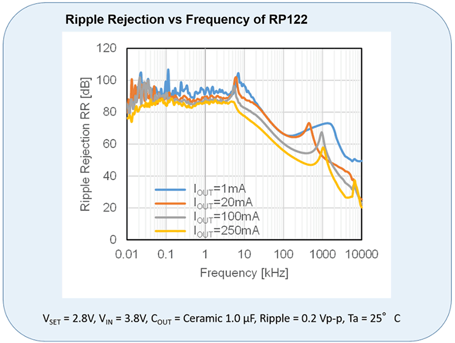
Figure 2. RP122's Industry-leading Ripple Rejection vs Frequency Characteristic
Transient Response
This characteristic indicates how long and to what extent abrupt fluctuations in the input voltage and/or output current affect the output voltage, and how long it takes to return to a stable operation.
Load transient response
Load transient response refers to the response characteristics of the output voltage fluctuation amplitude and the release time against abrupt load current variations. As is mentioned in the previous volume, a negative feedback circuit keeps a fixed output voltage by controlling the on-resistance of the output driver according to the sequential fluctuations of output voltage, feedback voltage and output of the error amplifier which are caused by load fluctuations. Like this, a negative feedback circuit operates each component in order, so there occur lags between voltage fluctuation detection and output voltage restoration by the time required for the negative feedback loop. This is expressed as the response speed of the negative feedback circuit. Abrupt load variations exceeding this response speed cause temporary drop or rise of the output voltage. After the response time has passed, the voltage restores to its set value. Figure 3 shows an example of load transient response.
Figure 3. Example of Load Transient Response Characteristic
Input transient response
Input transient response refers to the response characteristics of the output voltage fluctuation amplitude and the release time against abrupt input current variations.
Similarly to load transient response characteristics, abrupt input variations exceeding the response speed of a negative feedback circuit cause temporary drop or surge of the output voltage until the on-resistance of the output driver gets adjusted.
This is illustrated in Figure 4.
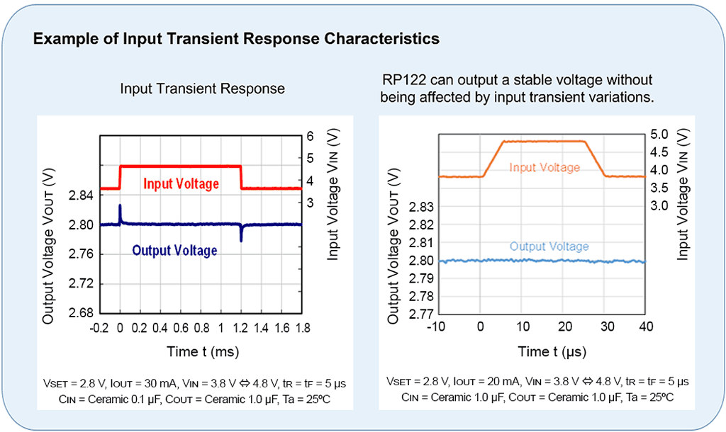
Figure 4. Example of Input Transient Response Characteristics
Supply Current of Linear Regulator
Supply current refers to the amount of operating current necessary for a device to remain functionally ready. This term does not include current supplied to other devices nor to operate other devices. Therefore, it is sometimes expressed as self current consumption.
Regarding CMOS-based linear regulators, supply current refers to that excluding the current flowing via the output driver transistor to the load. The current flowing to the controlling circuit in Figure 5 corresponds to self current consumption.
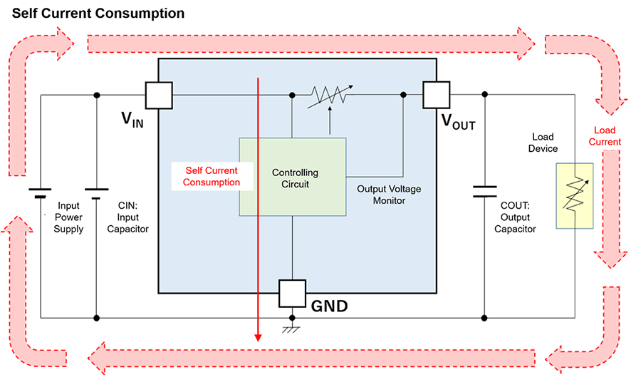
Figure 5. Self Current Consumption in Linear Regulator
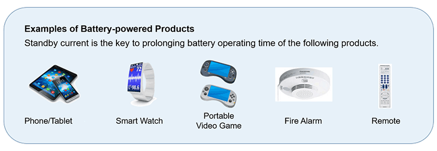
Figure 6. Applications that require Reduction in Standby Current to Prolong Battery Operating Time
Bipolar-based linear regulators require base current which never contributes to the load in order to supply current from the output driver to the load. A bipolar transistor constantly needs base current for its operation, and therefore it is difficult to reduce standby current of this current-driven transistor.
On the other hand, a CMOS-based linear regulator requires no such current thanks to its voltage-driven transistor. As a result, a CMOS-based regulator can easily achieve low self current consumption.
For example, CMOS regulators can reduce self current consumption to around 200 nA and supply 100 mA to the load at the same time.
Battery-powered applications shown in Figure 6, such as fire alarms, stay in a standby mode during most of their operating time. From the perspective of the power management IC, the load device rarely operates unless it detects a fire and sounds an alarm. Using CMOS-based linear regulators with low self current consumption is an optimal solution to prolong the battery operating time of these applications that operate mainly in a standby mode.
Relationship between Supply Current and Performance
Basically, there is a trade-off between 'supply current' and 'high frequency characteristics of ripple rejection and load transient response'. In other words, decreasing supply current sacrifices transient response and ripple rejection, and enhancing performance such as ripple rejection and transient response also increases supply current.
These days, however, many manufacturers have been developing linear regulators achieving the coexistence of low supply current, good ripple rejection and transient response by using various circuit techniques.
Internal Loss and Power Dissipation
A device generates heat and raises its own temperature by internally consuming power, which is called internal loss. The generated heat is dissipated by the package and the mounting board. Therefore, the internal temperature of a device depends on how much electricity the device consumes and how much heat the package and the board can radiate.
Also, there is a limitation to the maximum temperature for a device to maintain stable operation, so its power consumption is determined so that the temperature never exceeds the limit. This is called power dissipation.
You can find power dissipation values of each package which is mounted on a standard board in the datasheets.
Considering power dissipation is very important, as a linear regulator generates a stable, fixed voltage by consuming electricity and generating heat in its output driver transistor. Consideration of power dissipation is also necessary for DC/DC converters (switching regulators), so we will explain this topic in the next volume.
Protective Functions
The on-resistance of a linear regulator, especially that of an LDO regulator, can become lower than or equal to 1 Ω. If the output of the regulator becomes short-circuited, a large current beyond expectations may flow inside the regulator. As a result, the IC may damage itself by the heat it generates. To protect linear regulators from damage, they internally have many protection functions. Let me briefly introduce some of them.
Current limit
This protection function regulates current that exceeds the output current limit. Linear regulators maintain a fixed output voltage regardless of its load current increase until the load current reaches its output current limit. When the load current reaches the limit, the current limit circuit regulates it to its output current limit value.
Short-circuit protection
As mentioned above, a linear regulator reduces its output current to its current limit value when the output pin becomes short. At the same time, it narrows its output current limit value in proportion to the output voltage decrease with a short-circuit protection circuit. The output current will be limited to several dozens of mA as the output voltage decreases to 0 V.
In a current limit circuit, output voltage decrease leads to the increase in power loss of a linear regulator. To solve this problem, a short-circuit protection function reduces output current to suppress the power loss increase and prevents the regulator from being damaged by heat.
This type of protection is called, in association with the graph showing the relationship of the two protective functions, fold back protection.
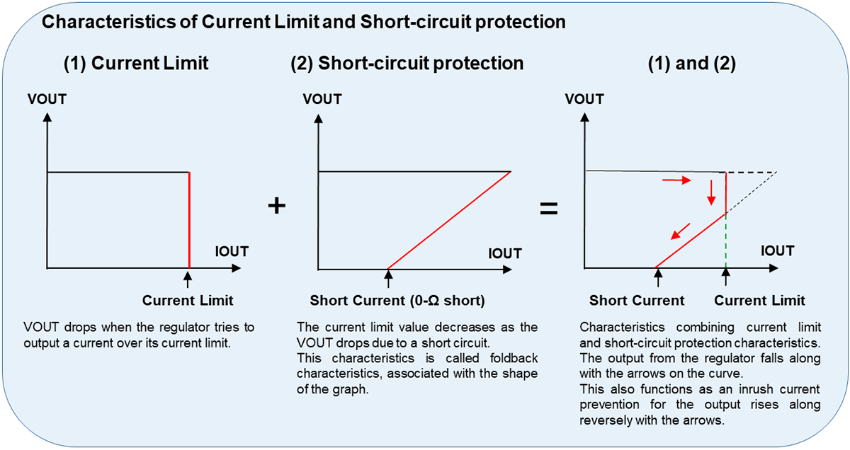
Figure 7. Relationship between Current Limit and Short-circuit Protection
The output voltage at the start-up of a linear regulator reaches its set voltage in the reverse order of fold back protection; namely, the short-circuit and current limit circuits also take the role of inrush current protection function.
Thermal Shutdown
A thermal shutdown function monitors the temperature of a linear regulator and protects it from being damaged by heat. When detecting a temperature exceeding the detection temperatures such as maximum junction temperature, the protective function stops the regulator's operation and turns off the output driver transistor to stop heat generation.
As the heat generation stops, the chip temperature will decrease. When the temperature reaches below the release temperature of the thermal shutdown function, the regulator will start to operate again.
However, without removing the cause of heat generation such as a short circuit in the output, the regulator would alternately repeat over-heat detection and restoration. In that case, this protective function cannot guarantee the reliability of the operation.
Input and Output Capacitors
At the beginning of Volume 2, I explained that a linear regulator can output a stable fixed voltage by using it with an input power supply, an input capacitor and an output capacitor. Then, what are the roles of these two capacitors? Here, I will introduce the role input and output capacitors play.
First, let us begin with output capacitors.
1. Output Capacitor
1) Improvement of Load Transient Response
As mentioned above, load transient response refers to the response characteristics of the output voltage fluctuation amplitude and the release time against abrupt load current variations.
We have explained in the previous volume that a negative feedback circuit keeps a fixed output voltage by controlling the on-resistance of the output driver according to the sequential fluctuations of output voltage, feedback voltage and output of the error amplifier which are caused by load fluctuations. A negative feedback circuit operates each component in order, so there occur lags between voltage fluctuation detection and output voltage restoration by the time required for negative feedback loop. This is expressed as the response speed of the negative feedback circuit. Abrupt load variations exceeding this response speed cause temporary output voltage drop.
The output capacitor plays a role of a temporary power supply to the load instead of the linear regulator, so as for the output voltage to not drop when the regulator is preparing to supply enough current corresponding to the load current increase.
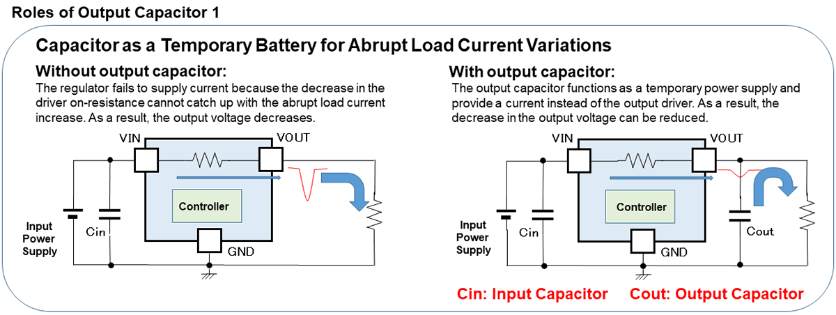
Figure 8. Output Capacitor as Temporary Battery for Abrupt Load Current Fluctuations
2) Phase Compensation
Most of the linear regulators use an output capacitor to conduct phase compensation. To do this, you need to use output capacitors whose operation with the regulator has been evaluated. Then, what is phase compensation?
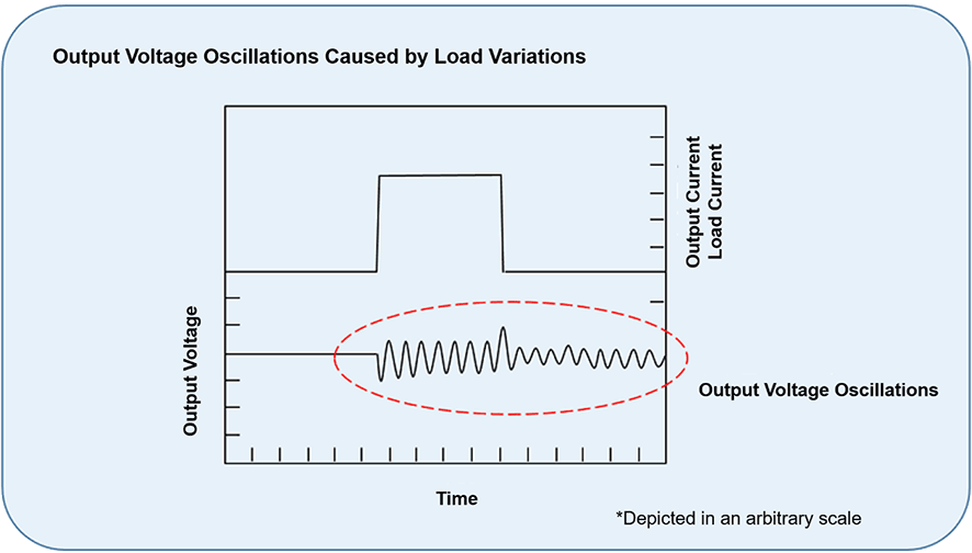
Figure 9. Output Voltage Oscillation Caused by Load Fluctuations
The waveform in Figure 9 illustrates transient output voltage oscillations caused by abrupt load current fluctuations. You can see that output voltage oscillations occur together with abrupt load current fluctuations. Why do such oscillations happen?
In the negative feedback circuit of a linear regulator, the error amplifier detects output voltage variations and controls the output voltage in the opposite direction to the variation. In other words, a negative feedback control circuit is controlled by signals whose phase differs from the output voltage variations by 180 degrees. However, the control delays by the time necessary for the circuit to operate. Specifically, a delay occurs between the time of the error amplifier detecting a variation and the time of a signal opposite to the variation reaching the error amplifier. This delay of time is called loop delay of a negative feedback circuit or phase shift. During gradual load variations this phase shift will not matter. However, in the case of abrupt load variations, output variations will also become abrupt, and phase shift cannot be ignored as frequency components become tremendously high.
Let us look at a case in which the error amplifier detects that the feedback voltage is higher than the reference voltage. The output variation can become lower than the reference voltage at the same time when an output voltage controlling signal which delays by the time of negative feedback loop reaches the error amplifier. In that case, the negative feedback operation which should suppress the output variations by controlling them in the opposite direction will amplify the variations due to phase shift. This phenomenon is called oscillations of a negative feedback loop, as shown in Figure 10.
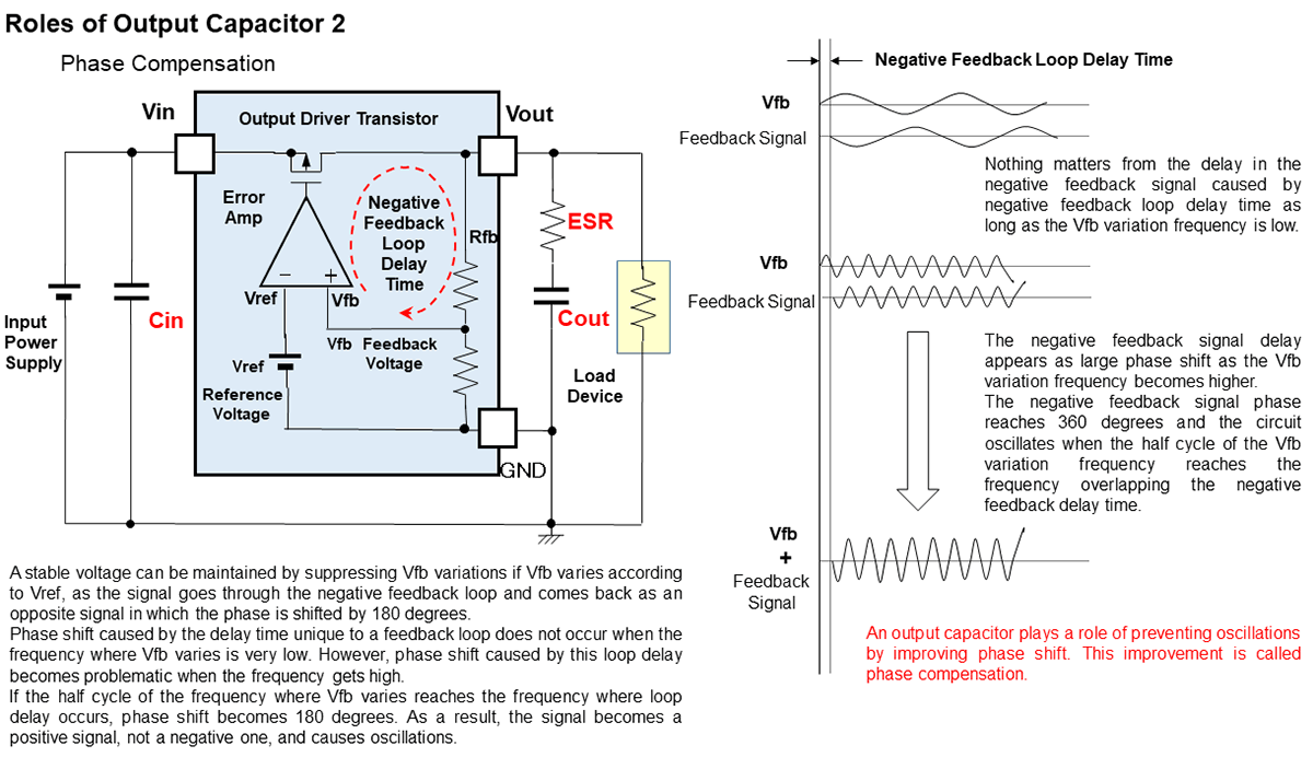
Figure 10. Oscillations in Negative Feedback Loop and Phase Compensation
Figure 10 illustrates that phase shift caused by the delay of the loop of 180 degrees if the frequency gets higher, is one of the conditions where oscillations occur.
On the other hand, there is another condition where oscillations occur: loop gain. Suppose a signal with a certain width and amplitude is input to an error amplifier. The signal goes through a negative feedback loop and returns to the error amplifier. Loop gain refers to the ratio of the returned signal width after going through the negative feedback loop to the input signal width.
As mentioned previously, phase shift occurs when the frequency gets higher inside a negative feedback loop, but at the same time loop gain decreases.
However, the loop gain of over one, or in other words, the returned signal width larger than the input signal width is the other condition where the output from the regulator results in oscillation.
Conversely, if loop gain is lower than 1, or, for instance, if the returned signal width is lower than 1 when an input signal with an oscillation width of 1 goes through the negative feedback loop and comes back, oscillations are attenuated and converged.
In summary, oscillations occur under the following conditions:
- The phase shift reaches 360 degrees and becomes positive feedback by 180-degree phase shift of circuit delay being added to 180-degree phase shift of a negative feedback loop circuit, or
- the loop gain of frequencies where phase delay reaches 180 degrees is 1 or more.
Conversely, if the loop gain of the negative feedback loop is lower than 1, oscillations never occur even during positive feedback loop.
To avoid oscillations, it is necessary to improve loop delay of the negative feedback circuit and to reduce loop gain below 1 for frequencies whose phase delay reaches 180 degrees.
Output capacitors, with their capacitance and equivalent series resistance (ESR), play an important role in improving phase delay.
In summary, phase compensation refers to suppression of the oscillations in a negative feedback circuit by improving phase delay of the negative feedback loop. Phase compensation of an LDO regulator is relatively easy to achieve by using an output capacitor with large capacitance and ESR; without using such a capacitor, it is very difficult for an LDO regulator to be adaptable to its actual usage while meeting all the requirements.
These days, linear regulators are designed with the premise of using a ceramic capacitor with small ESR of around 10 mΩ, so you need to check the datasheets of the products.
Then, let us go on to input capacitors.
2. Input Capacitor
Let us look at a linear regulator starting up. The output voltage is 0 V, and the COUT stores no charge. To charge the output capacitor COUT, a large current flow from the input pin via the output driver transistor and the output pin to the COUT in a short period of time, as if it started up from a short-circuit state. This large transient current flowing from the input to the output pins at a regulator's start-up is called inrush current. Without limiting it, a current of several amperes would flow transiently.
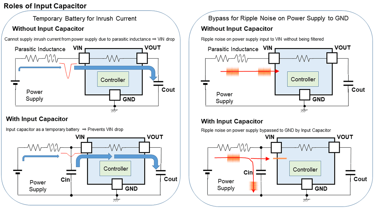
Figure 11. Roles of Input Capacitor
The power supply line powering the regulator has impedance like parasitic inductance and parasitic resistance, so transient current supply equal to the inrush current cannot catch up with it.
An input capacitor plays the role of a temporary power supply to cover a large current supply which an input power supply or a power management IC on the input side can never catch up with.
Without an input capacitor, the input voltage would drop steeply due to this inrush current and adversely affect operations of not only the linear regulator itself but also other devices which share that input power supply.
Also, an input capacitor decreases ripples by bypassing power supply fluctuations caused by operations of other devices on the power supply to the ground.
By the way, typical linear regulators have functions to limit output current at their starting up and to gradually raise output voltage. These functions suppress inrush current and prevent input voltage from dropping.
3. Selection and Mounting of Capacitors
When selecting capacitors, you need to take it into consideration that the capacitance varies depending on the pin voltage between input and output pins, which is called DC bias characteristics.
You may be able to find a list of capacitors whose operation with the linear regulator has been checked as per the datasheets. Especially, we recommend that you use one the ones listed in the datasheet for the output capacitor, as it is also used for phase compensation.
Also, in order for input and output capacitors to show their performance, you need to minimize the effects of parasitic resistance and parasitic inductance. To do this, put an input capacitor as close as possible to the VIN and GND pins, and an output capacitor as close as possible to the VOUT and GND pins.
Conclusion
In these two consecutive volumes, we have explained the mechanisms and specifications of linear regulators. We hope our explanation will help you understand principles and characteristics of linear regulators and choose the best one for your application.
In the next volume, we are going to talk about DC/DC converters (switching regulators) which can achieve not only buck but also boost and inverting operations. Also, we would like to explain efficiency of regulators we have not mentioned so far.
Thank you for reading.
Power Management IC Basics
- Vol. 1
What Are Power Management ICs? - Vol. 2
What Is a Linear Regulator (LDO Regulator)? Part 1 - Vol. 3
What Is a Linear Regulator (LDO Regulator)? Part 2 - Vol. 4
What Is a Linear Regulator (LDO Regulator)? Part 3 - Vol. 5
What Is a DC/DC Converter? Part 1 - Vol. 6
What Is a DC/DC Converter? Part 2 - Vol. 7
What Is a DC/DC Converter? Part 3 - Vol. 8
What Is a DC/DC Converter? Part 4 - Vol. 9
What Is a DC/DC Converter? Part 5 NEW
Author profile

Lecturer S (Nisshinbo Micro Devices Inc.)
For a long time since he joined the company, he has been involved in various analog and digital designs such as gate arrays, microcomputers, memories, and power management ICs. After that, he also mastered the test technology of compound power supply ICs and became a specialist in design, testing and education on his specialty. His easy-to-understand explanations and polite guidance from the listener's perspective are well received by new engineers who join our company every year. His achievements are highly commended, and now he is working as a senior engineer in training younger generations and as a consultant for new technologies.
FAQ: LDO Linear Regulators
- What is a soft-start function?
- Does the Reverse Current Protection Function of the R1191 work regardless of the CE status (H/L)?
- Regarding the output current of the NJM2871A, the maximum value is stated to be 150mA, but is there a minimum value?
- What is the input to CE pin when putting this series into standby state?
- How much is the value of CE pin's pull-down resistance of RP122?