


NJW4162A Series
2channel MOSFET Drive Switching Regulator IC for Buck Converter
NJW4162A Series
2channel MOSFET Drive Switching Regulator IC for Buck Converter


拡大
:q
Description
The NJW4162A is a 2 channel MOSFET Drive switching regulator IC for buck converter that operates wide input voltage range from 4.3V to 40V. The oscillating frequency range can set within 100kHz to 1MHz by external resistor. It also has an external synchronous function. It has individual Standby functions, Soft Start functions and Power Good functions for each channel, therefore a start-up control and/or operating condition monitoring are available with a microcomputer. The NJW4162A is suitable for a logic voltage generating circuit from high input voltage such as Automotive. Office Automation and Industrial applications.
Spec
| Standard | Automotive | |
|---|---|---|
| Input Voltage Range | 4.3 V to 40 V (45 V) | |
| Operating Temperature Range | -40°C to 125°C | |
| Supply Current | Typ. 4000 µA | Max. 6000 µA |
| Standby Current | 10 (max.) µA | |
| Output Voltage Range | 0.8 V to 38 V | |
| Output Voltage Accuracy | ± 1 % | ± 2 % |
| Oscillator Frequency | 100kHz to 1MHz | |
| Maximum Duty Cycle | 100% | |
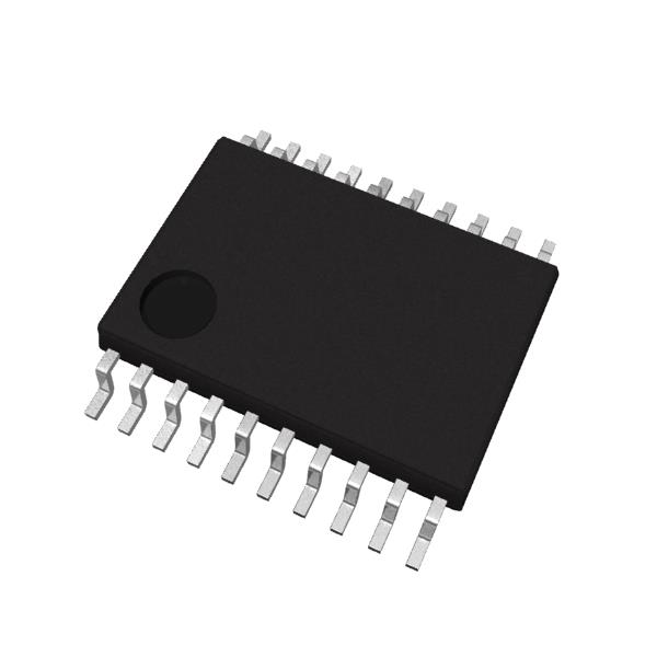
| Package | SSOP20-C3 | |
| Control | PWM Control | |
| Function | Standby Function Over Current Protection (Hiccup type) Thermal Shutdown Protection External Synchronization Function (1,500kHz (max.)) Power Good Function |
|
| Note | UVLO (Under Voltage Lockout) Adjustable Soft Start Function |
If you need datasheets of this product, please contact us. |
Protections / Functions
| TSD | OCP | OVP | UVLO | OVLO | Reverse | Shutdown | Soft Start | SSCG | PGOOD | Auto Discharge | Anti-ringing | Sequencing | Max Duty | Ext. Phase | LED Adjust |
|---|---|---|---|---|---|---|---|---|---|---|---|---|---|---|---|
 |
|
|
|
|
|
Functional Description
| TSD | Thermal Shutdown Function |
|---|---|
| OCP | Overcurrent Protection Note: The function previously labeled as "ILX (LX Current Limit Function)" is now shown as "OCP." |
| OVP | Overvoltage Protection |
| UVLO | Undervoltage Lockout Protection |
| OVLO | Overvoltage Lockout Protection |
| Reverse | Reverse Current Protection Circuit |
| Shutdown | Shutdown Function |
| Soft Start | Soft Start Function |
| SSCG | Spread Spectrum Clock Generator Function |
| PGOOD | Power Good Output |
| Auto Discharge | Auto Discharge Function |
| Anti-ringing | Anti-ringing Switch Function |
| Sequencing | Start-up Sequencing Control |
| Max Duty | Maximum Duty Cycle |
| Ext. Phase | Externally Adjustable Phase Compensation |
| LED Adjust | LED High-speed Dimming Control |
Technical Documents
-
Related Links
Quality & Packages
| Product Name | Compatibility | Package | Marking | Reliability |
|---|---|---|---|---|
| NJW4162AVC3 |
|
SSOP20-C3 | - | NJW-2a-s-fr |
| NJW4162AVC3-T1 |
|
SSOP20-C3 | - | NJW-2a-s-fr |

- Refer to the datasheets for the details on the product.
- The package file or the datasheet includes package dimensions, taping specifications, taping reels dimensions, power dissipations, and recommended land pattern.
FAQ
Buy / Contact
-
Purchase, Request for samples and documentsSales are made through distributors. Please contact your local distributors for any sales-related inquiry such as price.
-
Available from 1 piece!Our electronic device products are available through our authorized online distributors.
-
Technical Support
NJW4162A Series