


NJW4132 Series
Switching Regulator IC for Boost Converter Current Mode Control with 45V/1.75A MOSFET
NJW4132 Series
Switching Regulator IC for Boost Converter Current Mode Control with 45V/1.75A MOSFET


拡大
:q
Description
The NJW4132 is a boost converter with 45V/1.75A MOSFET. It corresponds to high oscillating frequency, and Low ESR Output Capacitor (MLCC) within wide input range from 4.5V to 40V.Therefore, the NJW4132 can realize downsizing of applications with a few external parts so that adopts current mode control.Also, it has a soft start function, external clock synchronization,over current protection and thermal shutdown circuit.It is suitable for boost application to a Car Accessory, Office Automation Equipment, Industrial Instrument and so on
Spec
| Standard | Automotive | |
|---|---|---|
| Input Voltage Range | 4.5 V to 40 V (45 V) | 4.55 V to 40 V (45 V) |
| Operating Temperature Range | -40°C to 85°C | -40°C to 125°C |
| Supply Current | Typ. 2000 µA | Typ. 3500 µA |
| Standby Current | 1 (max.) µA | |
| Output Voltage Range | 4.5 V to 40 V | 4.55 V to 40 V |
| Output Voltage Accuracy | ± 1 % | |
| Output Current | Switching Current 1750 mA | |
| Oscillator Frequency | 300kHz typ. (A ver.) / 700kHz typ. (B ver.) / 2.0MHz typ. (C ver.) | |
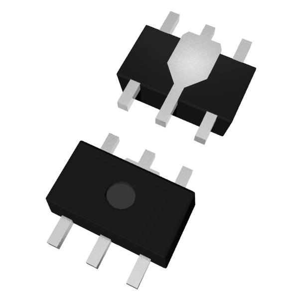
| Package | SOT-89-5-2 | |
| Control | Current Mode Control / PWM Control | |
| Function | Standby Function Soft Start Function (10ms typ.) Over Current Protection (Hiccup type) Thermal Shutdown Protection |
|
| Note | Built-in Compensation Circuit UVLO (Under Voltage Lockout) External Clock Synchronization Correspond to Ceramic Capacitor (MLCC) |
If you need datasheets of this product, please contact us. |
Protections / Functions
| TSD | OCP | OVP | UVLO | OVLO | Reverse | Shutdown | Soft Start | SSCG | PGOOD | Auto Discharge | Anti-ringing | Sequencing | Max Duty | Ext. Phase | LED Adjust |
|---|---|---|---|---|---|---|---|---|---|---|---|---|---|---|---|
 |
|
|
|
Functional Description
| TSD | Thermal Shutdown Function |
|---|---|
| OCP | Overcurrent Protection Note: The function previously labeled as "ILX (LX Current Limit Function)" is now shown as "OCP." |
| OVP | Overvoltage Protection |
| UVLO | Undervoltage Lockout Protection |
| OVLO | Overvoltage Lockout Protection |
| Reverse | Reverse Current Protection Circuit |
| Shutdown | Shutdown Function |
| Soft Start | Soft Start Function |
| SSCG | Spread Spectrum Clock Generator Function |
| PGOOD | Power Good Output |
| Auto Discharge | Auto Discharge Function |
| Anti-ringing | Anti-ringing Switch Function |
| Sequencing | Start-up Sequencing Control |
| Max Duty | Maximum Duty Cycle |
| Ext. Phase | Externally Adjustable Phase Compensation |
| LED Adjust | LED High-speed Dimming Control |
Technical Documents
-
SPICE model download
You can download the product's SPICE model. Login/registration to myNISD is required to download.
-
Related Links


Quality & Packages
| Product Name | Compatibility | Package | Marking | Reliability |
|---|---|---|---|---|
| NJW4132U2 |
|
SOT-89-5-2 | - | NJW-1-s-fr |
| NJW4132U2-C-T1 |
|
SOT-89-5-2 | - | NJW-1-s-fr |

- Refer to the datasheets for the details on the product.
- The package file or the datasheet includes package dimensions, taping specifications, taping reels dimensions, power dissipations, and recommended land pattern.
FAQ
Buy / Contact
-
Purchase, Request for samples and documentsSales are made through distributors. Please contact your local distributors for any sales-related inquiry such as price.
-
Available from 1 piece!Our electronic device products are available through our authorized online distributors.
-
Technical Support
NJW4132 Series