


NJW4122 Series
2A Synchronous Buck Converter for POL
NJW4122 Series
2A Synchronous Buck Converter for POL


拡大
:q
Description
The NJW4122 is a synchronous buck converter with 2A MOSFET. The NJW4122 has wide switching oscillating frequency range, 100kHz to 2.4MHz and external clock synchronization function. Therefore it can avoid interference with the AM radio frequency. Internal protection functions: UVLO, an over current protection and a thermal shutdown circuit can protect at abnormal condition. It is suitable for power supply circuit of SoC, DSP, DDR memory and so on that needs fast transient response.
Applications
- Power supply for SoC, ASIC, DDR and the others
Spec
| Standard | |
|---|---|
| Input Voltage Range | 2.7 V to 5.5 V (7 V) |
| Operating Temperature Range | -40°C to 125°C |
| Supply Current | Typ. 2200 µA |
| Standby Current | 1 (max.) µA |
| Output Voltage Range | 0.6 V to 5 V |
| Output Voltage Accuracy | ± 1 % |
| Output Current | 2000 mA |
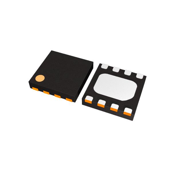
| Package | DFN8-U1(ESON8-U1) |
| Control | Current Mode Control PWM Control |
| Function | Standby Function Soft Start Function (1ms typ.) Over Current Protection (Hiccup type) Thermal Shutdown Protection |
| Note | UVLO (Under Voltage Lockout) Synchronous Rectification Correspond to Ceramic Capacitor (MLCC) |
Protections / Functions
| TSD | OCP | OVP | UVLO | OVLO | Reverse | Shutdown | Soft Start | SSCG | PGOOD | Auto Discharge | Anti-ringing | Sequencing | Max Duty | Ext. Phase | LED Adjust |
|---|---|---|---|---|---|---|---|---|---|---|---|---|---|---|---|
 |
|
|
|
|
|
Functional Description
| TSD | Thermal Shutdown Function |
|---|---|
| OCP | Overcurrent Protection Note: The function previously labeled as "ILX (LX Current Limit Function)" is now shown as "OCP." |
| OVP | Overvoltage Protection |
| UVLO | Undervoltage Lockout Protection |
| OVLO | Overvoltage Lockout Protection |
| Reverse | Reverse Current Protection Circuit |
| Shutdown | Shutdown Function |
| Soft Start | Soft Start Function |
| SSCG | Spread Spectrum Clock Generator Function |
| PGOOD | Power Good Output |
| Auto Discharge | Auto Discharge Function |
| Anti-ringing | Anti-ringing Switch Function |
| Sequencing | Start-up Sequencing Control |
| Max Duty | Maximum Duty Cycle |
| Ext. Phase | Externally Adjustable Phase Compensation |
| LED Adjust | LED High-speed Dimming Control |
Technical Documents
-
Related Links
Quality & Packages
| Product Name | Compatibility | Package | Marking | Reliability |
|---|---|---|---|---|
| NJW4122KU1 |
|
DFN8-U1(ESON8-U1) | - | NJW-1-s-r |

- Refer to the datasheets for the details on the product.
- The package file or the datasheet includes package dimensions, taping specifications, taping reels dimensions, power dissipations, and recommended land pattern.
FAQ
Buy / Contact
-
Purchase, Request for samples and documentsSales are made through distributors. Please contact your local distributors for any sales-related inquiry such as price.
-
Available from 1 piece!Our electronic device products are available through our authorized online distributors.
-
Technical Support
NJW4122 Series