


RP508 Series
600mA 6MHz PWM/VFM Step-down DC/DC Converter with Synchronous Rectifier


Description
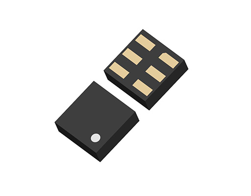
The RP508 Series are low supply current CMOS-based PWM/VFM step-down DC/DC converters with synchronous rectifier featuring 600mA* output current. The power controlling method can be selected from forced PWM control type or PWM/VFM auto switching control type by inputting a signal to the MODE pin. The RP508 includes a soft start circuit, an under-voltage lockout circuit (UVLO), a thermal shutdown circuit, and an auto-discharge function. The RP508 requires only a small numbers of external components to configure a high-efficiency step-up DC/DC converter: an inductor, capacitors and a diode as external components. The high-speed response corresponding to the high-speed switching frequency of 6MHz. The small-sized inductors (1.6 x 0.8 mm, 0.47µH) can be used. A 1.2-mm square compact DFN(PL)1212-6F package is available. *) This is an approximate value, because output current depending on conditions and external parts.
Spec
| Standard | |
|---|---|
| Input Voltage Range | 2.3 V to 5.5 V (6.5 V) |
| Operating Temperature Range | -40°C to 85°C (125°C) |
| Supply Current | Typ. 15 µA (VFM, no load) |
| Standby Current | Typ. 0 µA |
| Output Voltage Range | 0.8 V to 3.3 V (0.1 V step) |
| Output Voltage Accuracy | ±1.5% (VOUT ≥ 1.2 V, Ta = 25°C) ±18 mV (VOUT < 1.2 V) |
| Output Voltage Temperature Coefficient | Typ. ±100 ppm/°C |
| Output Current | 600 mA |
| Driver ON-resistance | Pch: Typ. 0.33 Ω, Nch: Typ. 0.24 Ω (VIN = 3.6 V) |
| Oscillator Frequency | Typ. 6.0 MHz |
| Maximum Duty Cycle | 100% |
| Package | DFN(PL)1212-6F |
Protections / Functions
| TSD | OCP | OVP | UVLO | OVLO | Reverse | Shutdown | Soft Start | SSCG | PGOOD | Auto Discharge | Anti-ringing | Sequencing | Max Duty | Ext. Phase | LED Adjust |
|---|---|---|---|---|---|---|---|---|---|---|---|---|---|---|---|
 |
|
|
|
|
Functional Description
| TSD | Thermal Shutdown Function |
|---|---|
| OCP | Overcurrent Protection Note: The function previously labeled as "ILX (LX Current Limit Function)" is now shown as "OCP." |
| OVP | Overvoltage Protection |
| UVLO | Undervoltage Lockout Protection |
| OVLO | Overvoltage Lockout Protection |
| Reverse | Reverse Current Protection Circuit |
| Shutdown | Shutdown Function |
| Soft Start | Soft Start Function |
| SSCG | Spread Spectrum Clock Generator Function |
| PGOOD | Power Good Output |
| Auto Discharge | Auto Discharge Function |
| Anti-ringing | Anti-ringing Switch Function |
| Sequencing | Start-up Sequencing Control |
| Max Duty | Maximum Duty Cycle |
| Ext. Phase | Externally Adjustable Phase Compensation |
| LED Adjust | LED High-speed Dimming Control |
Technical Documents
-
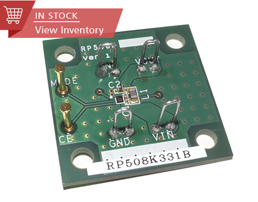
Evaluation Board
-
Typical Application
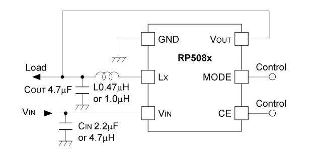
-
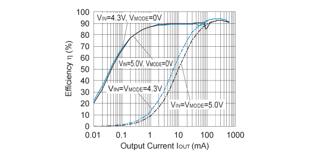
RP508K181x Efficiency vs. Output Current (VOUT=1.8V)
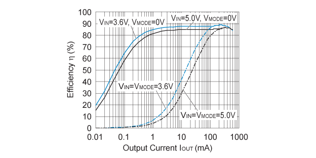
-
RP508K181x Efficiency vs. Output Current (VOUT=3.3V)
-
Related Links
Quality & Packages
| Product Name | Compatibility | Package | Marking | Reliability |
|---|---|---|---|---|
| RP508Kxx1x-TR |
|
DFN(PL)1212-6F | RP508K | RP508K |

- Refer to the datasheets for the details on the product.
- The package file or the datasheet includes package dimensions, taping specifications, taping reels dimensions, power dissipations, and recommended land pattern.
FAQ
Buy / Contact
-
Purchase, Request for samples and documentsSales are made through distributors. Please contact your local distributors for any sales-related inquiry such as price.
-
Available from 1 piece!Our electronic device products are available through our authorized online distributors.
-
Technical Support