


R1294 Series
Triple Output DC/DC Converter for LCD/CCD
R1294 Series
Triple Output DC/DC Converter for LCD/CCD


拡大
:q
Description
The R1294 Series are triple output CMOS-based step-up/inverting DCDC converters. R1294 consists of the inductor type PWM step-up DC/DC converter (DC/DC1) with an internal 2A Nch. driver and charge pump type positive/negative DCDC converters (DC/DC2, DC/DC3). Triple output start-up sequence can be set by external capacitors. R1294 is ideally suitable for use in power source for equipment that requires sequence control such as LCD and CCD. This product for industrial applications are characterized to -50°C, and operates in a wide temperature range from low temperature to high temperature.
Spec
| Standard | Industrial | Automotive | |
|---|---|---|---|
| Input Voltage Range | 2.0 V to 5.5 V (6.5 V) | ||
| Operating Temperature Range | -40°C to 95°C (125°C) | -40°C to 105°C (150°C) | -40°C to 105°C (150°C) |
| Supply Current | Typ. 3.5 mA | ||
| Standby Current | Typ. 0.1 µA | ||
| Output Voltage Range | Boost DC/DC: Max. 20 V (Externally Adjustable) | ||
| Feedback Voltage | 1.0 V | ||
| Feedback Voltage Accuracy | ±15 mV | ||
| Feedback Voltage Temperature Coefficient | Typ. ±150 ppm/°C | ||
| Driver ON-resistance | Typ. 150 mΩ | ||
| Oscillator Frequency | Typ. 210 kHz to 1.4 MHz (Externally Adjustable) | ||
| Maximum Duty Cycle | Externally Adjustable | ||
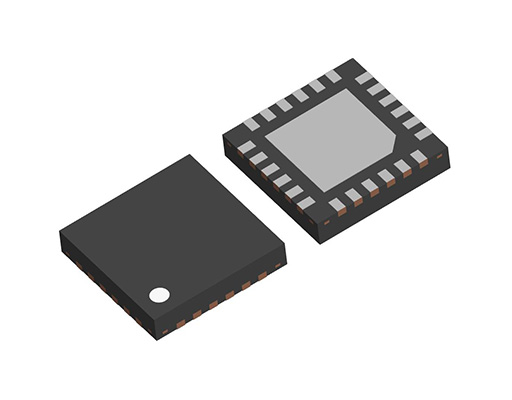
| Package | QFN0404-24B | ||
| Charge-pump Output Voltage | Adjustable with external resistors | ||
| Charge-pump Temperature Coefficient | VREF: Typ. ±150 ppm/°C CPPFB: Typ.±150 ppm/°C |
||
| Charge-pump Oscillator Frequency | 1/4 of the main step-up DC/DC converter oscillator frequency | ||
Protections / Functions
| TSD | OCP | OVP | UVLO | OVLO | Reverse | Shutdown | Soft Start | SSCG | PGOOD | Auto Discharge | Anti-ringing | Sequencing | Max Duty | Ext. Phase | LED Adjust |
|---|---|---|---|---|---|---|---|---|---|---|---|---|---|---|---|
 |
|
|
|
|
|
Functional Description
| TSD | Thermal Shutdown Function |
|---|---|
| OCP | Overcurrent Protection Note: The function previously labeled as "ILX (LX Current Limit Function)" is now shown as "OCP." |
| OVP | Overvoltage Protection |
| UVLO | Undervoltage Lockout Protection |
| OVLO | Overvoltage Lockout Protection |
| Reverse | Reverse Current Protection Circuit |
| Shutdown | Shutdown Function |
| Soft Start | Soft Start Function |
| SSCG | Spread Spectrum Clock Generator Function |
| PGOOD | Power Good Output |
| Auto Discharge | Auto Discharge Function |
| Anti-ringing | Anti-ringing Switch Function |
| Sequencing | Start-up Sequencing Control |
| Max Duty | Maximum Duty Cycle |
| Ext. Phase | Externally Adjustable Phase Compensation |
| LED Adjust | LED High-speed Dimming Control |
Technical Documents
-
Typical Application
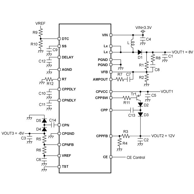
For external parts, please refer to the datasheet.
-
Related Links
Quality & Packages
| Product Name | Compatibility | Package | Marking | Reliability |
|---|---|---|---|---|
| R1294L10xA-E2 |
|
QFN0404-24B | R1294L | R1294L |
| R1294L10xA-E2-Y |
|
QFN0404-24B | R1294L | R1294L-Y |
| R1294L10xA-E2-J |
|
QFN0404-24B | R1294L | R1294L-J |
| R1294L10xA-E2-A |
|
QFN0404-24B | R1294L | R1294L-A |

- Refer to the datasheets for the details on the product.
- The package file or the datasheet includes package dimensions, taping specifications, taping reels dimensions, power dissipations, and recommended land pattern.
Qualification Test Plan (QTP) Sheets
To download the QTP sheets, a myNISD account is required. If you do not have an account, please register in advance.If you already have an account, please click the button below. After logging in to myNISD, the QTP sheet list page for the corresponding series will be displayed.
FAQ
Buy / Contact
-
Purchase, Request for samples and documentsSales are made through distributors. Please contact your local distributors for any sales-related inquiry such as price.
-
Available from 1 piece!Our electronic device products are available through our authorized online distributors.
-
Technical Support
R1294 Series