


R1273 Series
14A 34V Input Step-down DC/DC Converter with Synchronous Rectifier


Description
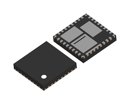
The R1273 is a step-down DC/DC converter which can generate an output voltage of 0.7 V to 5.3 V by driving high- / low-side NMOSs. By the adoption of a unique current mode PWM architecture without an external current sense resistor, the R1273 can make up a stable DC/DC converter with high-efficiency even if adding low Ron MOSFETs and a low DCR inductor externally. And, by the frequency characteristics optimization with using external phase compensation capacitor, the R1273 can achieve a high-speed response to variations of input voltage and load current. The user-settable oscillation frequency is adjustable over a range of 250 kHz to 1 MHz by external resistors, and also can be synchronized to an external clock in a range of 250 kHz to 1 MHz. The R1273 supports three operating modes: Forced PWM mode, PLL_PWM mode, and PWM/VFM Auto-switching mode. These modes are selectable according to conditions of the MODE pin. Especially, the PWM/VFM Auto-switching mode can improve efficiency under light load conditions. The R1273 can minimize the output voltage drop caused by an input voltage drop at cranking, with reducing the operating frequency (the lowest possible limit is a quarter of the frequency) so that the off-duty is reduced. Protection functions include a current limit function, a hiccup-mode short-circuit protection (non-latch type), a thermal shutdown function, an UVLO (Under Voltage Lock Out) function, an OVD (Over Voltage Detection) function, a soft-start function, a low-inductor current shutdown function, and so on. Also, a power good function provide the status of output with using a power good (PGOOD) pin. For EMI reduction, SSCG (Spread-Spectrum Clock Generator) for diffused oscillation frequency at the PWM operation is optionally available. The R1273 is available in QFN0505-32B package.
Spec
| Standard | Industrial | Automotive | |
|---|---|---|---|
| Input Voltage Range | 4.0 V to 34.0 V (36.0 V) | ||
| Operating Temperature Range | -40°C to 105°C (125°C) | -40°C to 105°C (125°C) | -40°C to 125°C (150°C) |
| Supply Current | Typ. 15 µA | ||
| Standby Current | Typ. 3 µA | ||
| Start-up Voltage | 4.5 V | ||
| Output Voltage Range | Externally Adjustable: 0.7 V to 5.3 V | ||
| Feedback Voltage | 0.64 V | ||
| Feedback Voltage Accuracy | ±1% | ||
| Driver ON-resistance | High-side: Typ. 11.8 mΩ / Low-side: Typ. 12.3 mΩ | ||
| Oscillator Frequency | Externally Adjustable: 250 kHz to 1 MHz | ||
| Package | QFN0505-32B | ||
Protections / Functions
| TSD | OCP | OVP | UVLO | OVLO | Reverse | Shutdown | Soft Start | SSCG | PGOOD | Auto Discharge | Anti-ringing | Sequencing | Max Duty | Ext. Phase | LED Adjust |
|---|---|---|---|---|---|---|---|---|---|---|---|---|---|---|---|
 |
|
|
|
|
|
|
|
Functional Description
| TSD | Thermal Shutdown Function |
|---|---|
| OCP | Overcurrent Protection Note: The function previously labeled as "ILX (LX Current Limit Function)" is now shown as "OCP." |
| OVP | Overvoltage Protection |
| UVLO | Undervoltage Lockout Protection |
| OVLO | Overvoltage Lockout Protection |
| Reverse | Reverse Current Protection Circuit |
| Shutdown | Shutdown Function |
| Soft Start | Soft Start Function |
| SSCG | Spread Spectrum Clock Generator Function |
| PGOOD | Power Good Output |
| Auto Discharge | Auto Discharge Function |
| Anti-ringing | Anti-ringing Switch Function |
| Sequencing | Start-up Sequencing Control |
| Max Duty | Maximum Duty Cycle |
| Ext. Phase | Externally Adjustable Phase Compensation |
| LED Adjust | LED High-speed Dimming Control |
Technical Documents
-
Typical Application
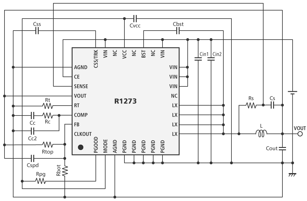
-
Efficiency vs. Output Current
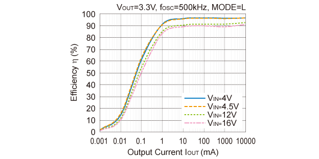
-
Related Links
Quality & Packages
| Product Name | Compatibility | Package | Marking | Reliability |
|---|---|---|---|---|
| R1273LxxxA-E2 |
|
QFN0505-32B | See datasheet | R1273L |
| R1273LxxxA-E2-Y |
|
QFN0505-32B | See datasheet | R1273L-Y |
| R1273LxxxA-E2-A |
|
QFN0505-32B | See datasheet | R1273L-A |

- Refer to the datasheets for the details on the product.
- The package file or the datasheet includes package dimensions, taping specifications, taping reels dimensions, power dissipations, and recommended land pattern.
FAQ
Buy / Contact
-
Purchase, Request for samples and documentsSales are made through distributors. Please contact your local distributors for any sales-related inquiry such as price.
-
Available from 1 piece!Our electronic device products are available through our authorized online distributors.
-
Technical Support