


NC4650 Series
Ultra-Low Quiescent Current (Iq = 70nA) Boost Switching Regulator with Low Ripple Mode
- Download Datasheet
- Point
-
Provides at-a-glance product features, functions, and concepts.
- ECAD Model: Learn more
-


Description
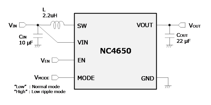
The NC4650 is a synchronous rectification boost switching regulator featuring ultra-low quiescent current of 70nA, utilizing a CMOS process. It is optimal for portable devices powered by coin or button batteries. With high efficiency under light load conditions, it is ideal for intermittent operation applications, ensuring long battery life. The MODE pin enables the selection of "Low Ripple Mode" for improved load transient response and reduced ripple. The EN pin allows shutdown operations, with options such as VIN-VOUT Complete Disconnect, VOUT discharge, and Pass-Through. Selecting the optimal version according to system sleep conditions enables system optimization.
Spec
| Standard | |
|---|---|
| Input Voltage Range | 0.6 V to 5.5 V (6.5 V) |
| Operating Temperature Range | TJ = -40°C to 125°C |
| Operating Quiescent Current | Normal Mode:Typ. 70 nA (Ta = 25°C) Low Ripple Mode:Typ. 90 µA (Ta = 25°C) |
| Output Voltage Range | 1.8 V to 5.0 V (0.1 V step) |
| Output Voltage Accuracy | ±1.5% (Ta = 25°C) |
| Switch Current Limit | Typ. 1000 mA (VSET ≥2.5 V) Typ. 650 mA (VSET <2.5 V) |
Protections / Functions
| TSD | OCP | OVP | UVLO | OVLO | Reverse | Shutdown | Soft Start | SSCG | PGOOD | Auto Discharge | Anti-ringing | Sequencing | Max Duty | Ext. Phase | LED Adjust |
|---|---|---|---|---|---|---|---|---|---|---|---|---|---|---|---|
 |
|
|
|
|
Functional Description
| TSD | Thermal Shutdown Function |
|---|---|
| OCP | Overcurrent Protection Note: The function previously labeled as "ILX (LX Current Limit Function)" is now shown as "OCP." |
| OVP | Overvoltage Protection |
| UVLO | Undervoltage Lockout Protection |
| OVLO | Overvoltage Lockout Protection |
| Reverse | Reverse Current Protection Circuit |
| Shutdown | Shutdown Function |
| Soft Start | Soft Start Function |
| SSCG | Spread Spectrum Clock Generator Function |
| PGOOD | Power Good Output |
| Auto Discharge | Auto Discharge Function |
| Anti-ringing | Anti-ringing Switch Function |
| Sequencing | Start-up Sequencing Control |
| Max Duty | Maximum Duty Cycle |
| Ext. Phase | Externally Adjustable Phase Compensation |
| LED Adjust | LED High-speed Dimming Control |
Technical Documents
-
Typical Application
-
Efficiency Typical Characteristics
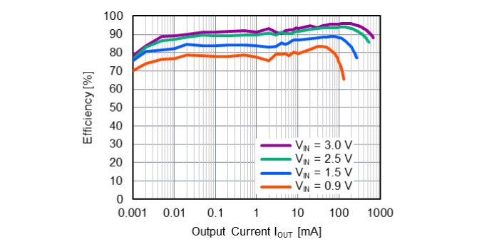
VOUT = 3.3 V, MODE = "Low"
-
Related Links
Quality & Packages
| Product Name | Compatibility | Package | Marking | Reliability |
|---|---|---|---|---|
| NC4650ZAxxxxE2S |
|
WLCSP-6-ZA1 | See Datasheet | NC4650ZAS |

- Refer to the datasheets for the details on the product.
- The package file or the datasheet includes package dimensions, taping specifications, taping reels dimensions, power dissipations, and recommended land pattern.
FAQ
Buy / Contact
-
Purchase, Request for samples and documentsSales are made through distributors. Please contact your local distributors for any sales-related inquiry such as price.
-
Available from 1 piece!Our electronic device products are available through our authorized online distributors.
-
Technical Support