


RF Switch (Radio Frequency Switch)
– Transmit RF signals as They Are –Connect Everything Wirelessly, Volume 5
– Transmit RF signals as They Are –Connect Everything Wirelessly, Volume 5

RF switches (radio-frequency switches) are used to switch the signal path of RF signals (radio-frequency signals); RF signals cannot communicate properly unless they are switched to the appropriate signal path configured for each communication standard and frequency band.
For example, smartphones can handle RF signals of various communication standards such as 5G, WiFi, and Bluetooth, and have multiple paths for filtering and amplification corresponding to each communication standard and frequency band. Furthermore, the transmit and receive paths may be different, requiring RF switches with many switching paths and multiple RF switches to switch RF signals transmitted and received via a limited number of antennas.
The figure below is a simplified version of the blocks that handle RF signals, as shown in the introduction to the first RF Device Series column.
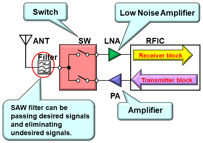
The RF switch shown in the figure is required to pass the RF signal from the antenna through the filter to the Low Noise Amplifier (LNA) side in receive mode, and to block the RF signal to the Power Amplifier (PA) side so as not to leak.
Then, in transmit mode, the RF signal sent from the transmitter is amplified by the PA, transmitted through the RF switch and filter to the antenna, and radiated from the antenna into the air.
Since the output power from the PA is greater than the RF signal power input to the RF switch in the receive mode, the RF switch must have characteristics that prevent RF signal leakage to the receive side in the transmit mode.
RF Switch Configuration
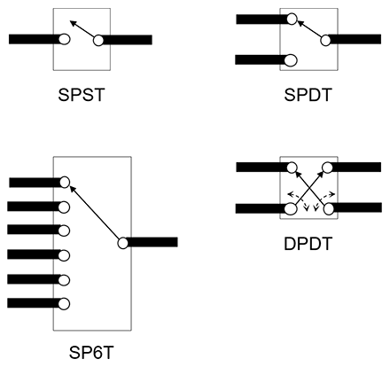
The configuration of RF switches is expressed by the number of input and output pins. The simplest one-input, one-output configuration is called Single-Pole Single-Throw (SPST), while the one-input, two-output configuration for switching between two paths is called Single-Pole Double-Throw (SPDT).
We offer a wide range of products from SPDT to SP6T and Double-Pole Double-Throw (DPDT), which switches between two inputs and two outputs.
RF switches that pass RF signals are required to have the performance of how well they can pass signals as they are without degradation. Specifically, power insertion loss, isolation which represents power leakage from the pass-through path, harmonic distortion and intermodulation distortion which represent signal distortion, and switching speed are the main RF characteristic items used to describe the capability of RF switches.
Configuration Examples of RF Switches
What makes RF switches different from other switch ICs?
There are various types of switch ICs with different functions and characteristics depending on the target application.
For example, our product lineup includes switch ICs that turn USB power lines on and off and control power distribution, analog switch ICs for switching analog signal paths, and audio switch ICs for switching audio signal paths.
So, for example, if we ask whether the aforementioned analog switch IC can switch the path of RF signals, the answer is it basically cannot. Probably, even if an RF signal is input to an analog switch IC that is not intended for RF signal use, little output power will be obtained. This is because the ON resistance, which is the resistance component of the path where the analog switch IC is ON, is too large for an RF switch.
First, transmission lines handling RF signals have a characteristic impedance of 50 Ω (75 Ω for video systems). Therefore, RF signals are transmitted and received with both the output impedance of the signal source and the load impedance of 50 Ω.
If the ON resistance of the switch IC connected in series to this 50 Ω transmission line is several hundred ohms, the voltage obtained at the load will be considerably reduced due to voltage division with the load resistance. If the Insertion Loss of the RF switch used in the 50 Ω system is to be kept below 0.5 dB, the ON resistance of the switch IC must be about 6 Ω or less.
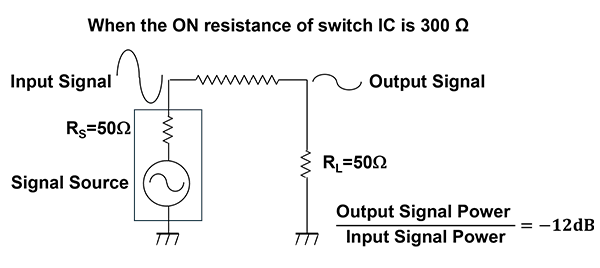
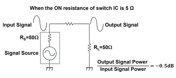
Calculation Example of Loss by On Resistance in 50 Ω System
However, this value is based on considering only the resistance component; in reality, the effects of parasitic inductance and parasitic capacitance in the path through the switch must also be considered.
RF signals, which have high frequencies ranging from several hundred MHz to several GHz, are affected in their transmission by various physical elements that become parasitic inductances and capacitances.
Even the depletion layer capacitance that occurs between the channel, drain, and source of the FET (Field Effect Transistor) that realizes the switching function and the semiconductor substrate can cause a loss of RF signal transmission power.
Not only that, various capacitances such as parasitic capacitances in the drain-source wiring of the FET that functions as an RF switch and fringe capacitances due to spatial coupling can work as OFF capacitance of the RF switch and cause RF signal loss.
RF switches are ICs with low ON resistance while suppressing parasitic components that cause such power loss.
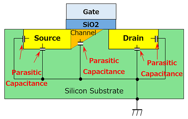
Parasitic Capacitance in Each Part of Silicon FET
RF Switch Devices
As mentioned above, RF switches require devices that can achieve low ON-resistance while suppressing parasitic components.
Originally, PIN diodes were used for RF signal switching, but with the advent of MESFETs, GaAs semiconductor RF switches took their place, and furthermore, with the advent of HEMTs*, even higher performance was realized, as described in the second volume of the RF Device columns.
(*HEMT: synonymous with HJFET, explained in the second volume.)
Then, why is it possible to achieve high performance RF switches by using HEMTs?
Electron Mobility
The first point to mention is that the electron mobility of HEMTs is very high.
The higher the carrier mobility, the lower the ON resistance of the FET. The electron mobility of HEMTs is much higher than that of silicon-based semiconductors, which means that HEMTs can achieve lower ON-resistance even with the same FET size. Since low ON-resistance can be achieved with a small FET size, the parasitic capacitance of the FET is also reduced, which further contributes to the suppression of transmission loss.
Semiconductor Resistivity
Next is the high resistivity of GaAs semiconductor substrates.
The resistivity of silicon-based substrates is generally between that of an insulator and a conductor, as they are called semiconductors. In reality, however, impurities are doped into the substrate, making the resistivity even lower than that of pure silicon.
In contrast, GaAs substrates have such high resistivity that they are called semi-insulators. When the substrate resistivity is high, the current flowing into the parasitic capacitance between the FET or wiring and the GaAs substrate is limited by the high resistance of the GaAs substrate, thus suppressing substrate losses.
These two main advantages are why HEMTs are used in high-performance RF switches.
However, silicon-based devices have also made great progress, and their performance as RF switches has dramatically improved due to shorter gate lengths and suppression of parasitic capacitance. In recent years, RF switches using silicon devices such as Silicon On Insulator (SOI) have become the mainstream, and we have also released SOI RF switches.
Performance Indicators of RF Switches
We have described the typical features of RF switches, and now we will briefly explain the specific RF performance indicators as described in the actual RF switch data sheets. (The names and descriptions of each index are based on our datasheets.)
- Insertion Loss
- The input-output ratio of the RF signal power passing through the RF switch. The smaller the value, the higher the performance.
- Isolation
- Ratio of power leaking from one RF signal path to another. The larger the value, the higher the performance.
- Return Loss
- Ratio of the input power to the RF switch to the reflected power. Sometimes expressed in terms of VSWR, in which case a smaller value indicates higher performance.
- Power at 0.1dB compression
- One of the linearity indices, the input power when the increase in insertion loss is 0.1 dB when the input power to the RF switch is increased. The larger the value, the higher the performance.
- Harmonics
- A measure of linearity, the power generated at integer multiples of the frequency of the input signal, respectively. The smaller the value, the higher the performance.
- Intermodulation Distortion
- A measure of linearity, the power generated at integer multiples of the frequency of the input signal, respectively. The smaller the value, the higher the performance.
- Switching Time
- Transition time from the input of the control signal for path switching to the convergence of the signal voltage of each path to the specified range when the path of the RF switch is switched. In most cases, the transition time for our RF switches is defined as the time when the RF voltage of the pass-through path becomes 90% or more of the steady state, or when the RF signal voltage of the pass-through path before switching becomes 10% or less of the steady state.
The above is a discussion of the functions of RF switches, the devices used, and the performance indicators needed when selecting RF switches.
Published Nov. 18, 2024
Authors' Profile
-

Hiroyuki Watari
With his experience in video amplifier design, he is an expert in RF circuits with knowledge of various circuits, both silicon and GaAs. He has contributed to the development of RF switch products mentioned in this column. He is also working on LNA design to further expand his field of activity, and is striving to realize advanced RF products.
-

Gaku Kato
Contributing to designing RF devices for over 20 years, including the development of the LNA achieving industry-leading low noise figure. With his motto "flexible product development that pleases customers," he devotes himself to creating prominent products. The representative of these columns.
Columns on RF Devices
Connect Everything Wirelessly
-
Rectifier Diodes for Wireless Power Transfer – To Realize a True Wireless Society –
-
RF Switch (Radio Frequency Switch) – Transmit RF signals as They Are –
-
Power Amplifier: The Key Device for Communication Applications
-
History of Our GaAs Semiconductor Products -History? Of Course There Is- (Latter Half)
-
History of Our GaAs Semiconductor Products -History? Of Course There Is- (Former Half)
-
Introduction: What Is a GaAs Semiconductor?
RF Device Related Information
Find Products
FAQ
- Are there any cases where DC blocking capacitors are required for RF switches not needing DC blocking capacitors connected to the RF terminals?
- I could not get the NF measurement value according to the datasheet. Please let us know how to resolve about this.
- Do you have low noise amplifiers (LNAs) for GNSS 1.2GHz band (L5/2/6 band)?
- In automotive GNSS, receiver sensitivity is degraded due to high cable losses in roof antenna applications. To compensate for this degradation, do you have a high-gain low noise amplifier for GNSS?
- Does latch-up occur in GaAs products?