


History of Our GaAs Semiconductor Products
-History? Of Course There Is- (Former Half) Connect Everything Wirelessly, Volume 2
-History? Of Course There Is- (Former Half) Connect Everything Wirelessly, Volume 2

New Japan Radio, a former company of Nisshinbo Micro Devices, started to mass-produce GaAs semiconductor products (integrated circuits) in 1995.
The first product mass-produced was an RF switch, which had a single input and switched two signal outputs.
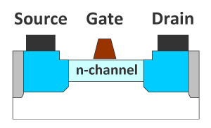
The transistors adopted a structure called MESFET*1.
*1 GaAs MESFET (Metal-Semiconductor Field Effect Transistor)
A MESFET is a kind of field effect transistor (FET). The gate structure of the FET is Schottky barrier junction formed by gate metals and the GaAs channel interface, which compose junction FETs. The channel part between the drain and source of the FET is formed by ion implantation, and generally it is an N-channel FET which can make use of the high speed of carriers.
The RF switch was used in personal handy-phone systems (PHS) which were a trend in Japan at that time. 1.9 GHz PHS used was the frequency bandwidth GaAs MESFETs were good at. Most of the time switches for PHS were GaAs semiconductors or PIN diodes at the time, but PIN diodes were replaced by GaAs RF switches gradually due to the current consumption: while PIN diodes consumed large current, GaAs RF switches were able to operate with low current consumption.
Many Japanese used them even in cities because they were smaller and cheaper than mobile phones at that time. The young people affectionately called them “pitch.” PHS are still widely used in hospitals and companies even today.
-
After that, the product field of our GaAs MESFET has become wider: in addition to RF switches, we have developed and manufactured power amplifiers, driver amplifiers, low noise amplifiers, mixers (frequency converters), and composite products. Furthermore, the applications using GaAs semiconductors were broadened to mobile phones, global positioning systems (GPS), etc. as well as PHS.
-
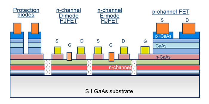
In 2000s, we developed products adopting new transistor structures called HJFET*2 and HBT*3. These new transistor structures contribute to enhancing the performance of GaAs semiconductor products, which have been released since 2000s.
*2 GaAs HJFET (Hetero-Junction Field Effect Transistor)
HJFETs are also a kind of FET called high-electron-mobility transistors which have complex channel structure compared to MESFETs. To put it simply, they are FETs of which donor-supply layer and channel layer are separated by an epitaxial layer with different composition. The gate is formed by Schottky barrier junction, the same with MESFETs.
HJFETs enhance electron mobility by forming an electron layer called two-dimensional electron gas which appears at the interface of the donor-supply layer and channel layer. This leads to radio frequency characteristics (cut-off frequency, noise figure) and reduction of channel resistance. As a result, HJFETs can achieve superior performance than MESFETs in these perspectives.
We can construct N-channel HJFETs suitable for RF switches and low noise amplifiers and P-channel HJFETs suitable for controller circuits, and are able to equip a compact single chip with a logic circuit and radio-frequency analog circuit.
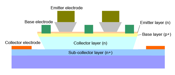
*3 GaAs HBT (Hetero-Junction Bipolar Transistor)
GaAs HBTs are a kind of bipolar transistor (BJT). We use GaAs for substrates and deposit epitaxial layers for collector, base and emitter layers which have a composition different from each other to form an N-P-N-structure BJT.
In the same way with silicon, for enhancement of the radio frequency characteristics of a BJT, especially cutoff frequency (fT) requires a thin base layer to shorten the transit time of a carrier, and high current gain (hFE) requires low carrier density in the base to increase emitter injection efficiency. However, there is a trade-off between the fT and maximum oscillation frequency (fmax), and between hFE and fmax in a conventional BJT; decreasing the thickness and density of the base layer increases the base resistance, which prevents increasing fmax.
In GaAs HBTs, this trade-off is solved by adopting an epitaxial layer with wider bandgap for the base than for the emitter to form an emitter-base heterojunction. This enables BJTs with high fmax to keep hFE without decreasing emitter injection efficiency even when the carrier density in the base is increased to decrease base resistance.
Silicon-based BJTs using heterojunction include SiGe HBTs which have different semiconductor materials but the same way to improve fT with GaAs. Nevertheless, the GaAs HBT process is more suitable for radio frequency applications than the Si process in the following perspectives: it can achieve higher electron mobility; and it can reduce leak current and parasitic capacitance in all elements including HBTs because elements are formed on a high-resistance substrate.
We use GaAs HBTs for power amplifier products because they can achieve higher current density per element layout area than HJFETs and therefore reduce the size of large-current devices.
“While the characteristics of GaAs semiconductors are good, I suspect they are vulnerable to static electricity.” This problem had been a big headache for RF system designers when choosing RF devices. We have produced GaAs semiconductor products tolerant to static electricity by adopting a protection diode developed through our unique technology. This contributes to reducing static electricity countermeasures on system boards of customers and thus leads to safe and secure products. New products with a protection diode have also been released since 2000s.
For example, when we produced to a customer a low-noise amplifier (LNA) with a gain switchover function for the front-end of a digital terrestrial television tuner, we contained a protection diode into the LNA. By offering the LNA and a protection circuit connected externally, the product could pass the 15-kV withstand voltage test of the IEC-61000-4-2 standard. Thanks to this protection diode technology, our LNAs are widely adopted to digital terrestrial televisions which need high static electricity tolerance.
Let us leave it there for this volume. In the next volume, the latter half of the history of our GaAs semiconductor products, we are going to talk mainly about packages.
Published Nov. 21, 2023
Authors' Profile
-

Kazushige Ikenaka
A specialist in R&D on RF devices who has devoted himself to planning and designing communication ICs since the car telephone era. He is also well versed in wireless communication systems, and establishes immense trust in internal technical lectures with his abundant knowledge and long experience.
-

Gaku Kato
Contributing to designing RF devices for over 20 years, including the development of the LNA achieving industry-leading low noise figure. With his motto "flexible product development that pleases customers," he devotes himself to creating prominent products. The representative of these columns.
Columns on RF Devices
Connect Everything Wirelessly
-
Rectifier Diodes for Wireless Power Transfer – To Realize a True Wireless Society –
-
RF Switch (Radio Frequency Switch) – Transmit RF signals as They Are –
-
Power Amplifier: The Key Device for Communication Applications
-
History of Our GaAs Semiconductor Products -History? Of Course There Is- (Latter Half)
-
History of Our GaAs Semiconductor Products -History? Of Course There Is- (Former Half)
-
Introduction: What Is a GaAs Semiconductor?
RF Device Related Information
Find Products
FAQ
- Are there any cases where DC blocking capacitors are required for RF switches not needing DC blocking capacitors connected to the RF terminals?
- I could not get the NF measurement value according to the datasheet. Please let us know how to resolve about this.
- Do you have low noise amplifiers (LNAs) for GNSS 1.2GHz band (L5/2/6 band)?
- In automotive GNSS, receiver sensitivity is degraded due to high cable losses in roof antenna applications. To compensate for this degradation, do you have a high-gain low noise amplifier for GNSS?
- Does latch-up occur in GaAs products?