


Introduction: What Is a GaAs Semiconductor?Connect Everything Wirelessly, Volume 1
Silicon (Si) is the most common element used for semiconductor products. It has long history as a material of semiconductor and is used in a wide range of applications and fields. Other semiconductor elements include germanium (Ge) and carbon (C), which are called single-elemental semiconductors.
On the other hand, there are also materials called compound semiconductors which include multiple elements, such as gallium arsenide (GaAs), indium phosphide (InP), gallium nitride (GaN), and so on. Compared to crystal of single element semiconductors, these compound semiconductors have more crystal defects and are broken more easily, so it is difficult to enlarge wafers of those materials. Also, another demerit is that compound semiconductors require more cost to obtain raw materials and manufacture them than Si semiconductors.
However, compound semiconductors have the advantage of high-speed signal processing compared to Si semiconductors. As electrons move faster inside compound semiconductors than inside Si, they are suitable for high-performance communication devices that deal with high-frequency signals. Therefore, GaAs semiconductors are widely used in communication devices such as cellular phones, base stations, and satellite communications.
-
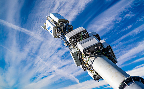
Base Stations
-

Satellite Communication
-
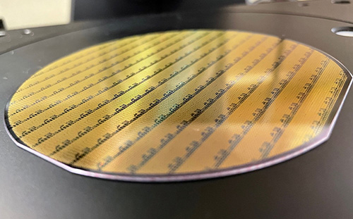
GaAs Semiconductor Wafer
GaAs semiconductors are contained in gadgets you use daily: for example, smartphones, smart watches, WiFi access points, Bluetooth earphones, digital terrestrial televisions, car navigation, etc.


We Nisshinbo Micro Devices have developed and manufactured GaAs semiconductor products for over 25 years. Our GaAs semiconductors work in the field of communication systems which are essential to our daily lives and today’s world.
For example, the following chart is a simplified diagram of a wireless communication system which contains a block dealing with radio frequency signals.
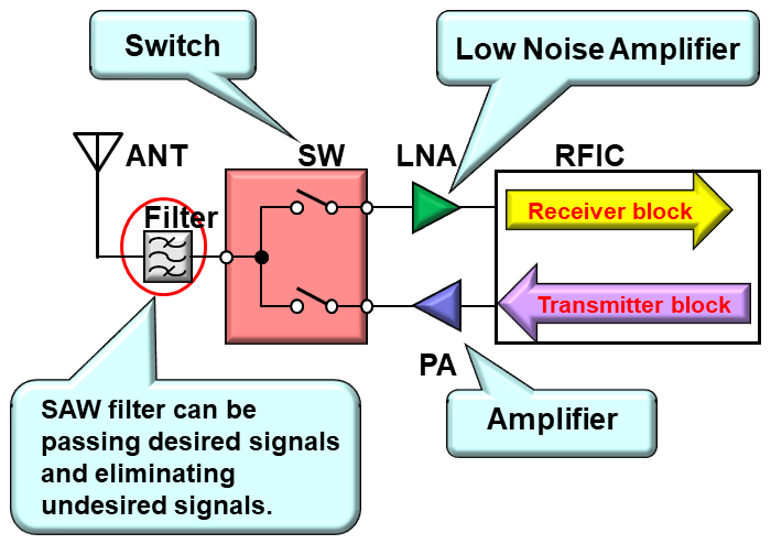
This block is composed of the following parts:
- An antenna to transmit and receive radio frequency signals (ANT);
- A filter to pass desired signals through and remove undesired signals (Filter);
- A switch to separate transmit and receive signals (SW);
- A power amplifier to amplify transmit signals (PA);
- A low noise amplifier to amplify receive signals (LNA);
- And a radio-frequency integrated circuit to process transmit/receive signals and communicate with the baseband block (RFIC).
These SW/LNA/PA products adopt GaAs semiconductors.
This web column on RF devices will give a series of technological topics mainly on GaAs semiconductors.
Published Nov. 21, 2023
Authors' Profile
-

Koji Hayashi
Having devoted himself to designing an array of RF devices since the start-up of our RF device business, he has a thorough knowledge of all the fields of RF devices. Also, he constantly collect information on the market and competitors to show what RF devices should aim at. He is relied on both internally and externally, and is highly skilled in solving any kinds of problems from customers.
-

Gaku Kato
Contributing to designing RF devices for over 20 years, including the development of the LNA achieving industry-leading low noise figure. With his motto "flexible product development that pleases customers," he devotes himself to creating prominent products. The representative of these columns.
Columns on RF Devices
Connect Everything Wirelessly
-
Rectifier Diodes for Wireless Power Transfer – To Realize a True Wireless Society –
-
RF Switch (Radio Frequency Switch) – Transmit RF signals as They Are –
-
Power Amplifier: The Key Device for Communication Applications
-
History of Our GaAs Semiconductor Products -History? Of Course There Is- (Latter Half)
-
History of Our GaAs Semiconductor Products -History? Of Course There Is- (Former Half)
-
Introduction: What Is a GaAs Semiconductor?
RF Device Related Information
Find Products
FAQ
- Are there any cases where DC blocking capacitors are required for RF switches not needing DC blocking capacitors connected to the RF terminals?
- I could not get the NF measurement value according to the datasheet. Please let us know how to resolve about this.
- Do you have low noise amplifiers (LNAs) for GNSS 1.2GHz band (L5/2/6 band)?
- In automotive GNSS, receiver sensitivity is degraded due to high cable losses in roof antenna applications. To compensate for this degradation, do you have a high-gain low noise amplifier for GNSS?
- Does latch-up occur in GaAs products?