


RP117 Series
Negative-voltage Low Noise 100mA LDO Regulator
RP117 Series
Negative-voltage Low Noise 100mA LDO Regulator
- Download Datasheet
- Point
-
Provides at-a-glance product features, functions, and concepts.
- ECAD Model: Learn more
-


拡大
:q
:q
Description
The RP117 is a negative voltage LDO regulator that provides high ripple rejection and low output noise. Adding only one capacitor to each input and output pin can make a simple structure and high performance LDO regulator.
Key Benefits
- Provides high ripple rejection rate and low output noise, which is ideal for noise-sensitive devices.
- Requires only one capacitor for each input and output pin, and is available in small DFN(PL)1212-6 and SC-88A packages, both of which can utilize the space on board.
Spec
| Standard | |
|---|---|
| Input Voltage Range | -10.0 V to -2.5 V (-11.0 V) |
| Operating Temperature Range | -40°C to 85°C (125°C) |
| Supply Current | Typ. 75 µA |
| Standby Current | Typ. 0.01 µA |
| Output Voltage Range | -5.5 V to -1.0 V (0.1 V step) |
| Output Voltage Accuracy | ±2.0% (Ta = 25°C, VSET ≤ -1.5 V), ±20 mV (VSET > -1.5 V) |
| Output Current | 100 mA |
| Ripple Rejection | Typ. 80 dB (f = 1 kHz) |
| Output Noise Voltage | Typ. 16 µVrms (VSET = −5.5 V ~ −2.0 V) |
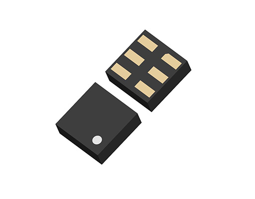
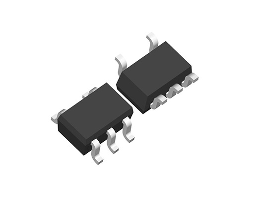
| Package | DFN(PL)1212-6, SC-88A |
Protections / Functions
| TSD | Reverse | Current Limit | ISC | Inrush | ECO mode | Auto Discharge | External Driver | PGOOD | Soft Start |
|---|---|---|---|---|---|---|---|---|---|
 |
|
|
|
Functional Description
| TSD | Thermal Shutdown Function |
|---|---|
| Reverse Current Protection | Reverse Current Protection |
| Current Limit | Overcurrent Protection |
| ISC | Short Current Protection |
| Inrush Current Limit | Inrush Current Protection |
| ECO mode | ECO Function |
| Auto Discharge | Auto Discharge Function |
| External Driver | External Output Driver Transistor |
| PGOOD | Power-Good |
| Soft Start | Soft Start Function |
Technical Documents
-
SPICE model download
You can download the product's SPICE model. Login/registration to myNISD is required to download.
-
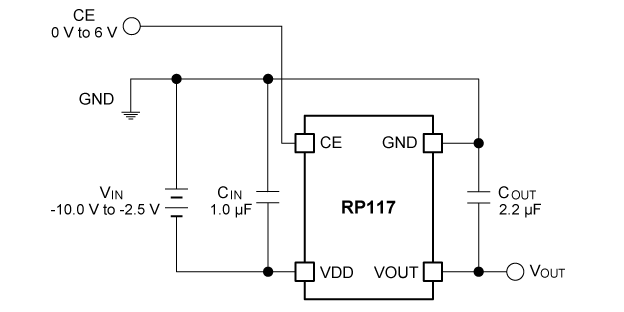
Typical Application
-
Ripple Rejection vs. Frequency
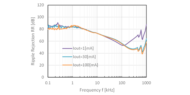
VSET = -1.0 V, VIN = -3.5 V, CIN = none, COUT = Ceramic 2.2 µF, Ripple = 0.2 Vp-p


Quality & Packages
| Product Name | Compatibility | Package | Marking | Reliability |
|---|---|---|---|---|
| RP117Kxx1D-TR |
|
DFN(PL)1212-6 | See datasheet | RP117K |
| RP117Qxx2D-TR-FE |
|
SC-88A | See datasheet | RP117Q-FE |

- Refer to the datasheets for the details on the product.
- The package file or the datasheet includes package dimensions, taping specifications, taping reels dimensions, power dissipations, and recommended land pattern.
FAQ
Buy / Contact
-
Purchase, Request for samples and documentsSales are made through distributors. Please contact your local distributors for any sales-related inquiry such as price.
-
Available from 1 piece!Our electronic device products are available through our authorized online distributors.
-
Technical Support
RP117 Series