


R5112 Series
Low Supply Current 42V Input 200mA Voltage Regulator with VD


Description
R5112 is an ultra-low supply current voltage regulator with a voltage detector featuring 200 mA output current and 42 V input voltage. This device consists of an Output Short-circuit Protection Circuit, an Overcurrent Protection Circuit, and a Thermal Shutdown Circuit in addition to the basic regulator circuits. It offers a wide range of operating temperature of −40°C to 105°C for consumer applications, and −40°C to 125°C for industrial and automotive applications. The maximum input voltage is 42 V. The output voltages are internally fixed at either of the following: 1.8 V, 2.5 V, 2.8 V, 3.0 V, 3.3 V, 3.4 V, or 5.0 V. The output voltage accuracy is ±0.6%. The detector threshold accuracy of the voltage detector is ±0.6%. This device is offered in an 8-pin HSOP-8E package with high power dissipation.
Spec
| Standard | Industrial | Automotive | |
|---|---|---|---|
| Input Voltage Range | 3.5 V to 42.0 V (50.0 V) | ||
| Operating Temperature Range | -40°C to 105°C (125°C) | -40°C to 125°C (150°C) | -40°C to 125°C (150°C) |
| Supply Current | Typ. 3.8 µA | ||
| Standby Current | Typ. 0.1 µA | ||
| Output Voltage Range | 1.8 V, 2.5 V, 2.8 V, 3.0 V, 3.3 V, 3.4 V, 5.0 V | ||
| Output Voltage Accuracy | ±0.6% (Ta = 25°C) | ||
| Output Voltage Temperature Coefficient | Typ. ±60 ppm/°C | ||
| Dropout Voltage | Typ. 0.6 V (IOUT = 200 mA, VSET = 5.0 V) | ||
| Line Regulation | Typ. 0.01%/V (2.5 V ≤ VSET: VSET + 1 V ≤ VIN ≤ 42 V) | ||
| Output Current | 200 mA | ||
| Package | HSOP-8E | ||
| Detector Threshold Range | B: 1.6 V to 4.8 V D: 2.9 V to 4.8 V |
||
| Detector Threshold Accuracy | ±0.6% (Ta = 25°C) | ||
| Detector Threshold Temperature Coefficient | Typ. ±60 ppm/°C | ||
Protections / Functions
| TSD | Reverse | Current Limit | ISC | Inrush | ECO mode | Auto Discharge | External Driver | PGOOD | Soft Start |
|---|---|---|---|---|---|---|---|---|---|
 |
|
|
Functional Description
| TSD | Thermal Shutdown Function |
|---|---|
| Reverse Current Protection | Reverse Current Protection |
| Current Limit | Overcurrent Protection |
| ISC | Short Current Protection |
| Inrush Current Limit | Inrush Current Protection |
| ECO mode | ECO Function |
| Auto Discharge | Auto Discharge Function |
| External Driver | External Output Driver Transistor |
| PGOOD | Power-Good |
| Soft Start | Soft Start Function |
Technical Documents
-
SPICE model download
You can download the product's SPICE model. Login/registration to myNISD is required to download.
-
R5112SxxxB Typical Application
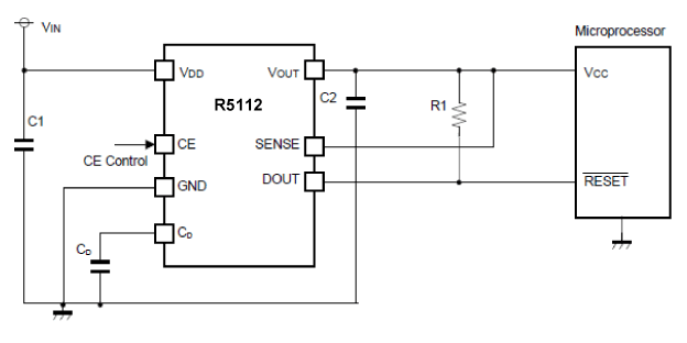
C1 (CIN), C2 (COUT) : 0.1 µF or more
-
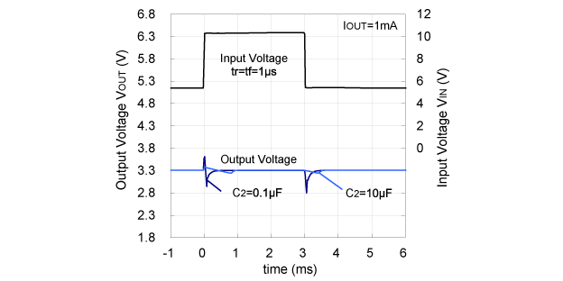
Input Transient Response


Quality & Packages

- Refer to the datasheets for the details on the product.
- The package file or the datasheet includes package dimensions, taping specifications, taping reels dimensions, power dissipations, and recommended land pattern.
Qualification Test Plan (QTP) Sheets
To download the QTP sheets, a myNISD account is required. If you do not have an account, please register in advance.If you already have an account, please click the button below. After logging in to myNISD, the QTP sheet list page for the corresponding series will be displayed.
FAQ
Buy / Contact
-
Purchase, Request for samples and documentsSales are made through distributors. Please contact your local distributors for any sales-related inquiry such as price.
-
Available from 1 piece!Our electronic device products are available through our authorized online distributors.
-
Technical Support