


RP510 Series
4A Forced PWM Step-down DC/DC Converter with Synchronous Rectifier
RP510 Series
4A Forced PWM Step-down DC/DC Converter with Synchronous Rectifier
- Download Datasheet
- Point
-
Provides at-a-glance product features, functions, and concepts.
- ECAD Model: Learn more
-


拡大
:q
Description
The RP510 is a step-down DCDC converter that operates the low input voltage of 2.5 V to 5.5 V. The RP510 being suitable for power supply of SoC (System-on-chip) can be output to 4 A (Max.). And, the foldback type protection, which be released automatically from the overcurrent protection, is user-selectable. This product for industrial applications are characterized to -50°C, and operates in a wide temperature range from low temperature to high temperature.
Key Benefits
- The realization of the high-density mounting by the adoption of a small package DFN3030-12
- A simplification of the power sequencing by power-good and adjustable soft-start functions
- Selectable overcurrent protection: Latch type or Foldback type
Spec
| Standard | Industrial | Automotive | |
|---|---|---|---|
| Input Voltage Range | 2.5 V to 5.5 V (6.5 V) | ||
| Operating Temperature Range | -40°C to 85°C (125°C) | -50°C to 105°C (150°C) | -40°C to 125°C (150°C) -40°C to 105°C (150°C) |
| Supply Current | Typ. 800 µA | ||
| Standby Current | RP510LxxxG/H/J : Typ. 0.01 µA以下 RP510LxxxN : Typ. 0.35 µA |
||
| Output Voltage Range | Internally Fixed Ver.: 0.8 V, 1.0 V, 1.1 V, 1.2 V, 1.3 V, 1.5 V, 1.8 V, 3.0 V, 3.3 V Externally Adjustable: 0.8 V to 3.3 V |
||
| Output Voltage Accuracy | ±1.0% (VSET ≥ 1.2 V, Ta = 25°C) ±12 mV (VSET < 1.2 V) |
||
| Feedback Voltage Accuracy | ±6 mV (VFB = 0.6 V) | ||
| Output Current | 4 A | ||
| Driver ON-resistance | Typ. 0.04 Ω (VIN = 3.6 V) | ||
| Oscillator Frequency | Typ. 2.3 MHz | ||
| Maximum Duty Cycle | Min. 100% | ||
| Package | DFN3030-12 | ||
Protections / Functions
| TSD | OCP | OVP | UVLO | OVLO | Reverse | Shutdown | Soft Start | SSCG | PGOOD | Auto Discharge | Anti-ringing | Sequencing | Max Duty | Ext. Phase | LED Adjust |
|---|---|---|---|---|---|---|---|---|---|---|---|---|---|---|---|
 |
|
|
|
|
|
Functional Description
| TSD | Thermal Shutdown Function |
|---|---|
| OCP | Overcurrent Protection Note: The function previously labeled as "ILX (LX Current Limit Function)" is now shown as "OCP." |
| OVP | Overvoltage Protection |
| UVLO | Undervoltage Lockout Protection |
| OVLO | Overvoltage Lockout Protection |
| Reverse | Reverse Current Protection Circuit |
| Shutdown | Shutdown Function |
| Soft Start | Soft Start Function |
| SSCG | Spread Spectrum Clock Generator Function |
| PGOOD | Power Good Output |
| Auto Discharge | Auto Discharge Function |
| Anti-ringing | Anti-ringing Switch Function |
| Sequencing | Start-up Sequencing Control |
| Max Duty | Maximum Duty Cycle |
| Ext. Phase | Externally Adjustable Phase Compensation |
| LED Adjust | LED High-speed Dimming Control |
Technical Documents
-
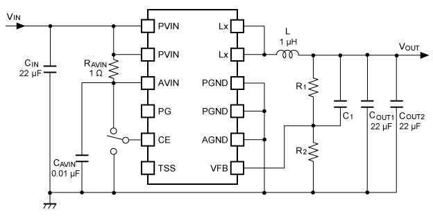
RP510L001J/1N/4J/4N Typical Application (Adjustable Output Voltage Type)
-
Efficiency vs. Output Current
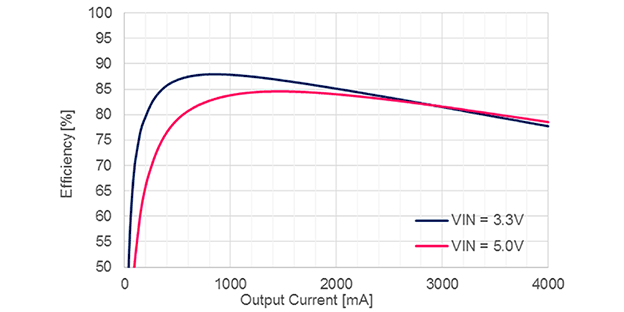
VOUT=1.2V, VIN=3.3V/5.0V
-
Related Links
Quality & Packages
| Product Name | Compatibility | Package | Marking | Reliability |
|---|---|---|---|---|
| RP510Lxxxx-TR |
|
DFN3030-12 | RP510L | RP510L |
| RP510Lxxxx-TR-Y |
|
DFN3030-12 | RP510L | RP510L-Y |
| RP510Lxxxx-TR-K |
|
DFN3030-12 | RP510L | RP510L-K |
| RP510Lxxxx-TR-A |
|
DFN3030-12 | RP510L | RP510L-A |

- Refer to the datasheets for the details on the product.
- The package file or the datasheet includes package dimensions, taping specifications, taping reels dimensions, power dissipations, and recommended land pattern.
Qualification Test Plan (QTP) Sheets
To download the QTP sheets, a myNISD account is required. If you do not have an account, please register in advance.If you already have an account, please click the button below. After logging in to myNISD, the QTP sheet list page for the corresponding series will be displayed.
FAQ
Buy / Contact
-
Purchase, Request for samples and documentsSales are made through distributors. Please contact your local distributors for any sales-related inquiry such as price.
-
Available from 1 piece!Our electronic device products are available through our authorized online distributors.
-
Technical Support
RP510 Series