


RP509 Series
0.5A/1A 6MHz PWM/VFM Step-down DC/DC Converter with Synchronous Rectifier
- Download Datasheet
- Point
-
Provides at-a-glance product features, functions, and concepts.
- ECAD Model: Learn more
-


Description
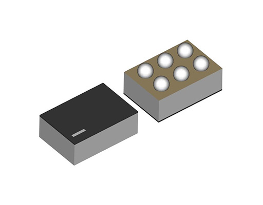
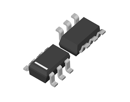
The RP509 is a low supply current PWM/VFM step-down DCDC converter with synchronous rectifier featuring 0.5A / 1A output current. Output voltage controlling method is selectable between a forced PWM control type and a PWM/VFM auto-switching control type, and can be set by the MODE pin. Internally, a single converter consists of a reference voltage unit, an error amplifier, a switching control circuit, a mode control circuit, a soft-start circuit, an under-voltage lockout (UVLO) circuit, a thermal shutdown circuit, and switching transistors. Furthermore, RP509 is current limit circuit and thermal shutdown circuit. Lx current limit value (Typ.) is selectable between 1.6 A and 1.0 A. The RP509Z is available in WLCSP−6−P6 which achieves high-density mounting on boards. A high frequency of 6 MHz enables to use capacitor of 0402- / 1005-size (inch / mm) and inductor of 0603- /1608-size (inch / mm) as external parts help to save space for devices.The RP509N is available in SOT-23-6.
Spec
| Standard | |
|---|---|
| Input Voltage Range | 2.3 V to 5.5 V (6.5 V) |
| Operating Temperature Range | -40°C to 85°C (125°C) |
| Supply Current | Typ. 15 µA |
| Standby Current | Typ. 0 µA |
| Output Voltage Range | Internally Fixed Ver.: 0.6 V to 3.3 V (0.1 V step) Externally Adjustable Ver.: 0.6 V to 5.5 V |
| Output Voltage Accuracy | ±1.5% (VSET ≥ 1.2 V, Ta = 25°C), ±18 mV (VSET < 1.2 V) |
| Output Voltage Temperature Coefficient | ±100 ppm/°C |
| Feedback Voltage | 0.6 V |
| Feedback Voltage Accuracy | ±9 mV |
| Feedback Voltage Temperature Coefficient | ±100 ppm/°C |
| Output Current | 0.5 A, 1 A |
| Driver ON-resistance | Pch: Typ. 0.175 Ω, Nch; Typ. 0.155 Ω (RP509Z) Pch: Typ. 0.195 Ω, Nch: Typ. 0.175 Ω (RP509N) |
| Oscillator Frequency | Typ. 6 MHz |
| Maximum Duty Cycle | Min. 100% |
| Package | WLCSP-6-P6, SOT-23-6 |
Protections / Functions
| TSD | OCP | OVP | UVLO | OVLO | Reverse | Shutdown | Soft Start | SSCG | PGOOD | Auto Discharge | Anti-ringing | Sequencing | Max Duty | Ext. Phase | LED Adjust |
|---|---|---|---|---|---|---|---|---|---|---|---|---|---|---|---|
 |
|
|
|
|
Functional Description
| TSD | Thermal Shutdown Function |
|---|---|
| OCP | Overcurrent Protection Note: The function previously labeled as "ILX (LX Current Limit Function)" is now shown as "OCP." |
| OVP | Overvoltage Protection |
| UVLO | Undervoltage Lockout Protection |
| OVLO | Overvoltage Lockout Protection |
| Reverse | Reverse Current Protection Circuit |
| Shutdown | Shutdown Function |
| Soft Start | Soft Start Function |
| SSCG | Spread Spectrum Clock Generator Function |
| PGOOD | Power Good Output |
| Auto Discharge | Auto Discharge Function |
| Anti-ringing | Anti-ringing Switch Function |
| Sequencing | Start-up Sequencing Control |
| Max Duty | Maximum Duty Cycle |
| Ext. Phase | Externally Adjustable Phase Compensation |
| LED Adjust | LED High-speed Dimming Control |
Technical Documents
-
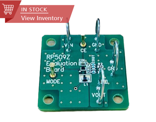
Evaluation Board
-
Typical Application (Fixed Output Voltage Type)
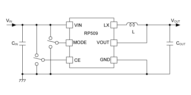
CIN: 4.7 µF
COUT: 10 µF
L: 0.47 µH -
Typical Application (Adjustable Output Voltage Type)
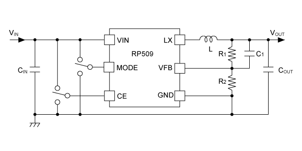
CIN: 4.7 µF
COUT: 10 µF
L: 0.47 µH -
Efficiency vs. Output Current VOUT=1.8V, VMODE = "L" PWM/VFM Auto Switching
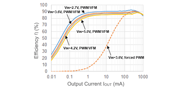
VOUT=1.8V VMODE = "L"
-
Efficiency vs. Output Current VOUT=3.3V Fixed, VMODE = "L" PWM/VFM Auto Switching
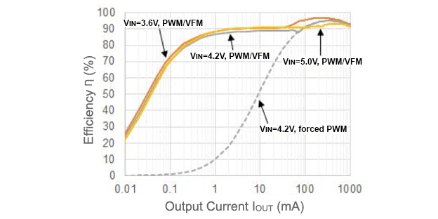
VOUT=3.3V VMODE = "L"
-
Related Links
Quality & Packages
| Product Name | Compatibility | Package | Marking | Reliability |
|---|---|---|---|---|
| RP509Zxxxx-E2-F |
|
WLCSP-6-P6 | See datasheet | RP509Z-F |
| RP509Nxxxx-TR-FE |
|
SOT-23-6 | See datasheet | RP509N-FE |

- Refer to the datasheets for the details on the product.
- The package file or the datasheet includes package dimensions, taping specifications, taping reels dimensions, power dissipations, and recommended land pattern.
FAQ
Buy / Contact
-
Purchase, Request for samples and documentsSales are made through distributors. Please contact your local distributors for any sales-related inquiry such as price.
-
Available from 1 piece!Our electronic device products are available through our authorized online distributors.
-
Technical Support