RP509 系列
0.5A/1A 6MHz带同步整流器功能的PWM/VFM降压DC/DC转换器


概述
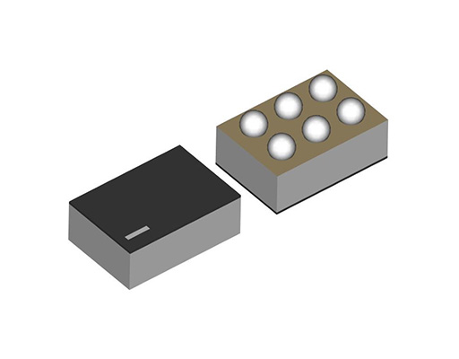
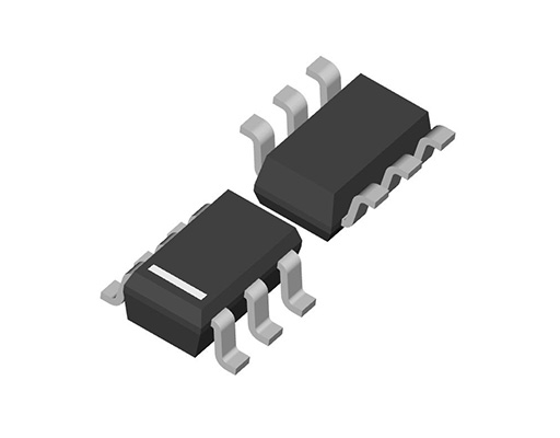
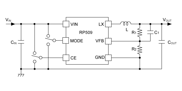
The RP509 is a low supply current PWM/VFM step-down DCDC converter with synchronous rectifier featuring 0.5A / 1A output current. Output voltage controlling method is selectable between a forced PWM control type and a PWM/VFM auto-switching control type, and can be set by the MODE pin. Internally, a single converter consists of a reference voltage unit, an error amplifier, a switching control circuit, a mode control circuit, a soft-start circuit, an under-voltage lockout (UVLO) circuit, a thermal shutdown circuit, and switching transistors. Furthermore, RP509 is current limit circuit and thermal shutdown circuit. Lx current limit value (Typ.) is selectable between 1.6 A and 1.0 A. The RP509Z is available in WLCSP−6−P6 which achieves high-density mounting on boards. A high frequency of 6 MHz enables to use capacitor of 0402- / 1005-size (inch / mm) and inductor of 0603- /1608-size (inch / mm) as external parts help to save space for devices.The RP509N is available in SOT-23-6.
规格
| 消费 | |
|---|---|
| 输入电压范围 | 2.3 V to 5.5 V (6.5 V) |
| 工作温度范围 | -40°C to 85°C (125°C) |
| 电源电流 | Typ. 15 µA |
| 待机电流 | Typ. 0 µA |
| 输出电压范围 | Internally Fixed Ver.: 0.6 V to 3.3 V (0.1 V step) Externally Adjustable Ver.: 0.6 V to 5.5 V |
| 输出电压精度 | ±1.5% (VSET ≥ 1.2 V, Ta = 25°C), ±18 mV (VSET < 1.2 V) |
| 输出电压温度系数 | ±100 ppm/°C |
| 反馈电压 | 0.6 V |
| 反馈电压精度 | ±9 mV |
| 反馈电压温度系数 | ±100 ppm/°C |
| 输出电流 | 0.5 A, 1 A |
| 驱动器导通电阻 | Pch: Typ. 0.175 Ω, Nch; Typ. 0.155 Ω (RP509Z) Pch: Typ. 0.195 Ω, Nch: Typ. 0.175 Ω (RP509N) |
| 振荡器频率 | Typ. 6 MHz |
| 最大占空比 | Min. 100% |
| 封装 | WLCSP-6-P6, SOT-23-6 |
保护回路/功能
| TSD | OCP | OVP | UVLO | OVLO | Reverse | Shutdown | Soft Start | SSCG | PGOOD | Auto Discharge | Anti-ringing | Sequencing | Max Duty | Ext. Phase | LED Adjust |
|---|---|---|---|---|---|---|---|---|---|---|---|---|---|---|---|
 |
|
|
|
|
功能说明
| TSD | 热关断电路 |
|---|---|
| OCP | 过流保护 注:以前标记为“ILX”的功能现在改为“OCP”。 |
| OVP | 过压保护 |
| UVLO | 欠压锁定功能 |
| OVLO | Overvoltage Lockout Protection |
| Reverse | 反向电流保护电路 |
| Shutdown | 关机功能 |
| Soft Start | 软启动功能 |
| SSCG | Spread Spectrum Clock Generator Function |
| PGOOD | Power Good Output |
| Auto Discharge | 自动放电功能 |
| Anti-ringing | Anti-ringing Switch Function |
| Sequencing | Start-up Sequencing Control |
| Max Duty | 最大占空比 |
| Ext. Phase | 外部可调相位补偿 |
| LED Adjust | LED High-speed Dimming Control |
技术资料
-
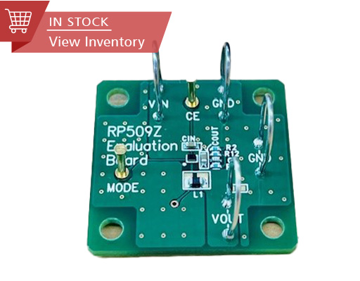
Evaluation Board
-
Typical Application (Fixed Output Voltage Type)
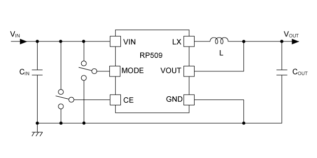
CIN: 4.7 µF
COUT: 10 µF
L: 0.47 µH -
Typical Application (Adjustable Output Voltage Type)
CIN: 4.7 µF
COUT: 10 µF
L: 0.47 µH -
Efficiency vs. Output Current VOUT=1.8V, VMODE = "L" PWM/VFM Auto Switching
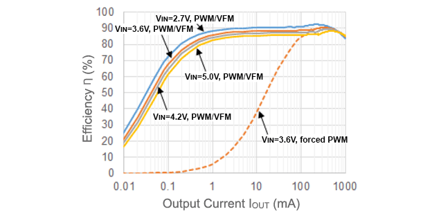
VOUT=1.8V VMODE = "L"
-
Efficiency vs. Output Current VOUT=3.3V Fixed, VMODE = "L" PWM/VFM Auto Switching
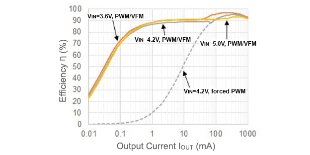
VOUT=3.3V VMODE = "L"
-
相关信息
品质・封装
| 产品名称 | 对应 | 封装 | 标注 | 信赖性 |
|---|---|---|---|---|
| RP509Zxxxx-E2-F |
|
WLCSP-6-P6 | 请参见数据表 | RP509Z-F |
| RP509Nxxxx-TR-FE |
|
SOT-23-6 | 请参见数据表 | RP509N-FE |

- 有关产品的详细信息,请参见数据表。
- 封装文件或数据表包括封装尺寸,卷带规格,卷带盘尺寸,功耗和建议的焊盘图案。
常问问题
购买 / 联系我们
-
技术支持