


R5524 Series
USB High-side Power Switch / Load Switch


Description
The R5524 Series is a CMOS-based high-side MOSFET switch IC which conforms to the universal serial bus (USB) standard. It can also be used as a load switch IC with protection function. By using an Nch MOSFET with low On-resistance (Typ. 100 mΩ) as a switching transistor, the device can provide low dropout voltage. Internally, the device consists of an overcurrent limiting circuit, a thermal shutdown circuit, an undervoltage lockout (UVLO) circuit and a reverse current protection circuit. The device also consists of an internal delay circuit to prevent the output of false flag signals caused by inrush current. To achieve simplification of layout design, the overcurrent detection accuracy has been improved.
Spec
| Standard | Industrial | Automotive | |
|---|---|---|---|
| Input Voltage Range | 2.7 V to 5.5 V (6.0 V) | ||
| Operating Temperature Range | -40°C to 85°C (125°C) | -40°C to 105°C (125°C) | -40°C to 85°C (125°C) |
| Supply Current | Typ. 110 µA | ||
| Standby Current | Typ. 0.1 µA | ||
| Output Current | Min. 550 mA | ||
| ON-resistance | Typ. 100 mΩ (VIN = 5 V) | ||
| Internal FET | Nch | ||
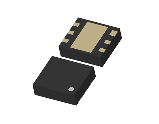
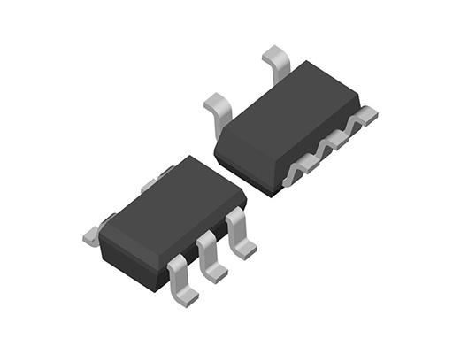
| Package | DFN(PL)1820-6, SOT-23-5 | DFN(PL)1820-6, SOT-23-5 | SOT-23-5 |
| Current Limit Threshold | Min. 650 mA (R5524x001A/B, R5524x002A/B) Min. 1.25 A (R5524N004A) |
||
| FLAG Delay Time | Typ. 20 ms | ||
| Thermal Shutdown | 135°C | ||
Protections / Functions
| TSD | Reverse | OCP | UVLO | OVLO | Soft Start | PGOOD | Auto Discharge | Reset |
|---|---|---|---|---|---|---|---|---|
 |
|
|
|
|
|
|
Functional Description
| TSD | Thermal Shutdown Function |
|---|---|
| Reverse Current Protection | Reverse Current Protection |
| OCP | Overcurrent Protection |
| UVLO | Undervoltage Lockout Protection |
| OVLO | Overvoltage Lockout Protection |
| Soft Start | Soft Start Function |
| PGOOD | Power Good Output |
| Auto Discharge | Auto Discharge Circuit |
Technical Documents
-
SPICE model download
You can download the product's SPICE model. Login/registration to myNISD is required to download.
-
Typical Application
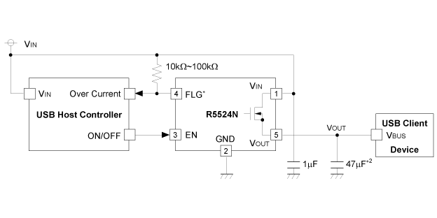
*) FLG pin is Nch. open drain output.
*2) For the USB standard, the capacitor value of 120µF or more must be connected with the output pin. -
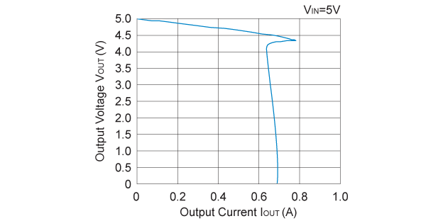
R5524x001x Output Voltage vs. Output Current


Quality & Packages
| Product Name | Compatibility | Package | Marking | Reliability |
|---|---|---|---|---|
| R5524N00xx-TR-FE |
|
SOT-23-5 | See datasheet | R5524N-FE |
| R5524K00xx-TR |
|
DFN(PL)1820-6 | See datasheet | R5524K |
| R5524N00xx-TR-YE |
|
SOT-23-5 | See datasheet | R5524N-YE |
| R5524K00xx-TR-Y |
|
DFN(PL)1820-6 | See datasheet | R5524K-Y |
| R5524N00xx-TR-AE |
|
SOT-23-5 | See datasheet | R5524N-AE |

- Refer to the datasheets for the details on the product.
- The package file or the datasheet includes package dimensions, taping specifications, taping reels dimensions, power dissipations, and recommended land pattern.
FAQ
Buy / Contact
-
Purchase, Request for samples and documentsSales are made through distributors. Please contact your local distributors for any sales-related inquiry such as price.
-
Available from 1 piece!Our electronic device products are available through our authorized online distributors.
-
Technical Support