


R5117 Series
42V Input Voltage Regulator with Battery Voltage Detector
R5117 Series
42V Input Voltage Regulator with Battery Voltage Detector
- Download Datasheet
- Point
-
Provides at-a-glance product features, functions, and concepts.
- ECAD Model: User Guide
-


拡大
:q
:q
Description
The R5117 is a power management IC featuring input voltage range from 3.5 V to 42 V. This IC includes battery voltage detector, SENSE voltage detector and 500 mA voltage regulator in a single chip. This IC can be used under high temperature environment. It offers the maximum operating temperature of 105°C for consumer applications, and 125°C for industrial and automotive applications. This product for industrial applications is characterized to −50°C, and operates in a wide temperature range from low temperature to high temperature.
Key Benefits
- Reducing components and improving functional safety
- The battery voltage detector suitable for early warning system against battery voltage reduction
- Preventing the false detection of transient characteristic fluctuations by high-speed response voltage regulator
Spec
| Standard | Industrial | Automotive | |
|---|---|---|---|
| Input Voltage Range | 3.5 V to 42.0 V (50.0 V) | ||
| Operating Temperature Range | -40°C to 105°C (125°C) | -50°C to 125°C (150°C) | -40°C to 125°C (150°C) |
| Supply Current | Typ. 35 µA | ||
| Standby Current | Typ. 10 µA | ||
| Output Voltage Range | 3.3 V to 5.0 V | ||
| Output Voltage Accuracy | ±0.5% (Ta = 25°C) -1.25% to 0.75% (−40°C ≤ Ta ≤ 105°C) |
±0.5% (Ta = 25°C) -1.25% to 0.75% (−50°C ≤ Ta ≤ 125°C) |
±0.5% (Ta = 25°C) -1.25% to 0.75% (−40°C ≤ Ta ≤ 125°C) |
| Output Current | 500 mA | ||
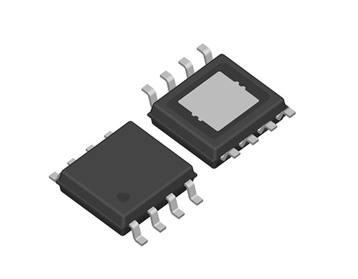
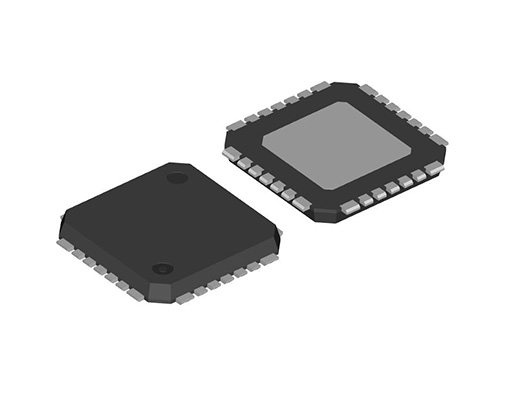
| Package | HSOP-8E, HQFN0808-28 | ||
| Detector Threshold Range | Sense Voltage Detection (SVD): 2.5 V to 5.0 V (0.01 V step) Battery Voltage Detection (BVD): 3.5 V to 12.0 V (0.1 V step) |
||
| Detector Threshold Accuracy | SVD: -1.25% to 0.75% BVD: -2.0% to 1.0% (−40°C ≤ Ta ≤ 105°C) |
SVD: -1.25% to 0.75% BVD: -2.0% to 1.0% (−50°C ≤ Ta ≤ 125°C) |
SVD: -1.25% to 0.75% BVD: -2.0% to 1.0% (−40°C ≤ Ta ≤ 125°C) |
| Release Hysteresis | SVD: Max. 0.7% BVD: Max. 5.0% |
||
Protections / Functions
| TSD | Reverse | Current Limit | ISC | Inrush | ECO mode | Auto Discharge | External Driver | PGOOD | Soft Start |
|---|---|---|---|---|---|---|---|---|---|
 |
|
|
Functional Description
| TSD | Thermal Shutdown Function |
|---|---|
| Reverse Current Protection | Reverse Current Protection |
| Current Limit | Overcurrent Protection |
| ISC | Short Current Protection |
| Inrush Current Limit | Inrush Current Protection |
| ECO mode | ECO Function |
| Auto Discharge | Auto Discharge Function |
| External Driver | External Output Driver Transistor |
| PGOOD | Power-Good |
| Soft Start | Soft Start Function |
Technical Documents
-
Typical Application
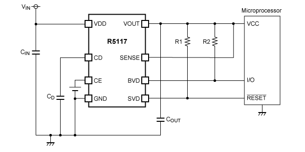
CIN: 1.0 µF, COUT: 10 µF, Ceramic capacitors
CD: Ceramic capacitors for setting detection delay time
Quality & Packages
| Product Name | Compatibility | Package | Marking | Reliability |
|---|---|---|---|---|
| R5117SxxxA-E2-FE |
|
HSOP-8E | R5117S | R5117S-FE |
| R5117LxxxA-TR-FE |
|
HQFN0808-28 | R5117L | R5117L-FE |
| R5117SxxxA-E2-YE |
|
HSOP-8E | R5117S | R5117S-YE |
| R5117LxxxA-TR-YE |
|
HQFN0808-28 | R5117L | R5117L-YE |
| R5117SxxxA-E2-AE |
|
HSOP-8E | R5117S | R5117S-AE |
| R5117SxxxA-E2-KE |
|
HSOP-8E | R5117S | R5117S-KE |
| R5117LxxxA-TR-AE |
|
HQFN0808-28 | R5117L | R5117L-AE |
| R5117LxxxA-TR-KE |
|
HQFN0808-28 | R5117L | R5117L-KE |

- Refer to the datasheets for the details on the product.
- The package file or the datasheet includes package dimensions, taping specifications, taping reels dimensions, power dissipations, and recommended land pattern.
Qualification Test Plan (QTP) Sheets
To download the QTP sheets, a myNISD account is required. If you do not have an account, please register in advance.If you already have an account, please click the button below. After logging in to myNISD, the QTP sheet list page for the corresponding series will be displayed.
FAQ
Buy / Contact
-
Purchase, Request for samples and documentsSales are made through distributors. Please contact your local distributors for any sales-related inquiry such as price.
-
Available from 1 piece!Our electronic device products are available through our authorized online distributors.
-
Technical Support
R5117 Series