


R1210 Series
8V Input PWM Step-up DC/DC Converter


Description
The R1210 Series are low supply current, CMOS-based PWM step-up DC/DC converters. By simply using an inductor, a diode, and a capacitor as external components, a high-efficiency step-up DC/DC converter can be easily configured. The xx1 version with an internal output transistor and the xx2 version with an external transistor are available. The oscillator frequency can be selected from 100kHz or 180kHz. The xx1A version is also available, which contains a basic frequency changeover circuit that switches the oscillator frequency from 100kHz to 35kHz when output load is reduced. R1210 also has a function that detects drastic changes in output voltage and reduces the amount of overshoot/undershoot by switching control mode.
Spec
| Standard | |
|---|---|
| Input Voltage Range | 0.8 V to 8.0 V (9.0 V) |
| Operating Temperature Range | -40°C to 85°C (125°C) |
| Supply Current | Typ. 10 µA |
| Standby Current | Typ. 0.5 µA |
| Start-up Voltage | Max. 0.9 V (R1210Nxx1x) Max. 0.8 V (R1210Nxx2x) |
| Output Voltage Range | 2.2 V to 3.5 V (0.1 V step) (R1210Nxx1A) 2.2 V to 6.0 V (0.1V step) (R1210NxxxC/D) |
| Output Voltage Accuracy | ±2.5% (Ta = 25°C) |
| Output Voltage Temperature Coefficient | Typ. ±100 ppm/°C |
| Oscillator Frequency | 100 kHz (R1210Nxx1A, R1210NxxxC) 180 kHz (R1210NxxxD) |
| Efficiency | Typ. 88% (VIN = Set Output Voltage ×0.6 [V], IOUT = 10 mA) |
| Package | SOT-23-5 |
Protections / Functions
| TSD | OCP | OVP | UVLO | OVLO | Reverse | Shutdown | Soft Start | SSCG | PGOOD | Auto Discharge | Anti-ringing | Sequencing | Max Duty | Ext. Phase | LED Adjust |
|---|---|---|---|---|---|---|---|---|---|---|---|---|---|---|---|
 |
Functional Description
| TSD | Thermal Shutdown Function |
|---|---|
| OCP | Overcurrent Protection Note: The function previously labeled as "ILX (LX Current Limit Function)" is now shown as "OCP." |
| OVP | Overvoltage Protection |
| UVLO | Undervoltage Lockout Protection |
| OVLO | Overvoltage Lockout Protection |
| Reverse | Reverse Current Protection Circuit |
| Shutdown | Shutdown Function |
| Soft Start | Soft Start Function |
| SSCG | Spread Spectrum Clock Generator Function |
| PGOOD | Power Good Output |
| Auto Discharge | Auto Discharge Function |
| Anti-ringing | Anti-ringing Switch Function |
| Sequencing | Start-up Sequencing Control |
| Max Duty | Maximum Duty Cycle |
| Ext. Phase | Externally Adjustable Phase Compensation |
| LED Adjust | LED High-speed Dimming Control |
Technical Documents
-
R1210Nxx1x Typical Application
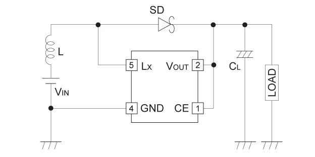
L: 100µH, CL: 22µFx2
-
R1210Nxx2x Typical Application
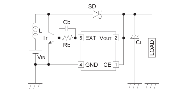
L: 27µH, CL: 47µF×2, Rb: 300Ω, Cb: 0.01µF
-
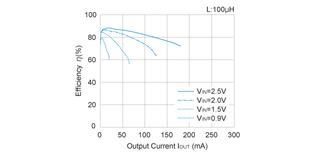
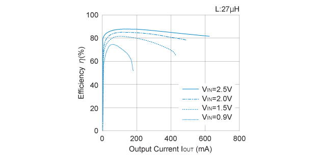
R1210N301C Efficiency vs. Output Current
-
R1210N302C Efficiency vs. Output Current
-
Related Links
Quality & Packages

- Refer to the datasheets for the details on the product.
- The package file or the datasheet includes package dimensions, taping specifications, taping reels dimensions, power dissipations, and recommended land pattern.
FAQ
Buy / Contact
-
Purchase, Request for samples and documentsSales are made through distributors. Please contact your local distributors for any sales-related inquiry such as price.
-
Available from 1 piece!Our electronic device products are available through our authorized online distributors.
-
Technical Support