


R5541 Series
18mΩ ON Resistance 3A Load Switch IC


Description
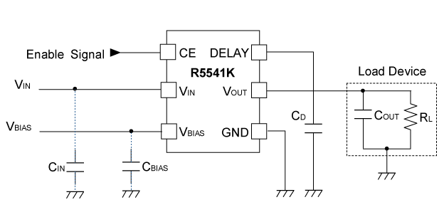
The R5541K is a CMOS-based dual supply voltage load switch IC. The R5541K is an ideal switch for supplying the power from the secondary power source such as the output of a step-down DC/DC converter to the load circuit. A built-in Nch. transistor with typically 18 mΩ ON resistance allows the R5541K to provide a low dropout voltage. Reverse current blocking function prevents the reverse current during shutdown mode. Internally, a single IC consists of an internal voltage step-up circuit, a soft-start circuit, a thermal shutdown circuit, a chip enable circuit and a UVLO circuit. The gate voltage of Nch. driver transistor is supplied by a soft-start circuit. The soft-start circuit is supplied by the external power source (VBIAS). Soft-start time is adjustable by connecting an external capacitor. The R5541K is offered in an ultra-small 6-pin DFN(PL)1216-6G package which achieve the smallest possible footprint solution on boards where area is limited.
Spec
| Standard | |
|---|---|
| Input Voltage Range | 0.6 V to 4.8 V (5.5 V) |
| Operating Temperature Range | -40°C to 85°C (125°C) |
| Supply Current | Typ. 25 µA (IOUT = 0 mA) |
| Standby Current | Typ. 0.01 µA |
| Output Current | Max. 3 A |
| ON-resistance | 18 mΩ (VIN = 1.0 V, VBIAS = 5.0 V) |
| Internal FET | Nch |
| Package | DFN(PL)1216-6G |
| VBIAS Input Voltage Range (Maximum Rating) | 2.5 V to 5.5 V (6.0 V) |
| Thermal Shutdown | 145°C |
Protections / Functions
| TSD | Reverse | OCP | UVLO | OVLO | Soft Start | PGOOD | Auto Discharge | Reset |
|---|---|---|---|---|---|---|---|---|
 |
|
|
|
|
Functional Description
| TSD | Thermal Shutdown Function |
|---|---|
| Reverse Current Protection | Reverse Current Protection |
| OCP | Overcurrent Protection |
| UVLO | Undervoltage Lockout Protection |
| OVLO | Overvoltage Lockout Protection |
| Soft Start | Soft Start Function |
| PGOOD | Power Good Output |
| Auto Discharge | Auto Discharge Circuit |
Technical Documents
-
SPICE model download
You can download the product's SPICE model. Login/registration to myNISD is required to download.
-
Typical Application
-
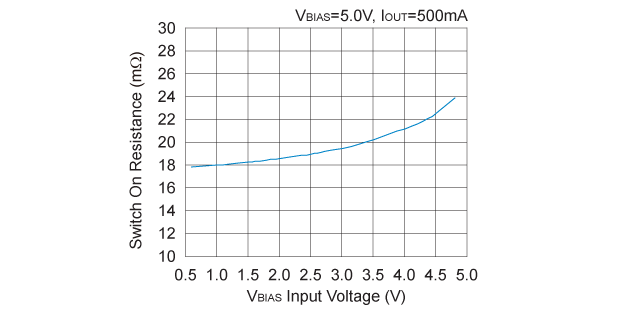
Switch On Resistance vs. VIN Input Voltage
-
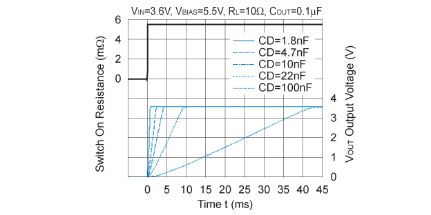
VOUT Output Voltage On Time vs. DELAY Capacitance


Quality & Packages
| Product Name | Compatibility | Package | Marking | Reliability |
|---|---|---|---|---|
| R5541K001x-E2 |
|
DFN(PL)1216-6G | See datasheet | R5541K |

- Refer to the datasheets for the details on the product.
- The package file or the datasheet includes package dimensions, taping specifications, taping reels dimensions, power dissipations, and recommended land pattern.
FAQ
Buy / Contact
-
Purchase, Request for samples and documentsSales are made through distributors. Please contact your local distributors for any sales-related inquiry such as price.
-
Available from 1 piece!Our electronic device products are available through our authorized online distributors.
-
Technical Support