


NV3600 Series
CMOS Output, Voltage Detector with High Withstand of SENSE Pin
NV3600 Series
CMOS Output, Voltage Detector with High Withstand of SENSE Pin
- Download Datasheet
- Point
-
Provides at-a-glance product features, functions, and concepts.
- ECAD Model: Learn more
-


拡大
:q
Description
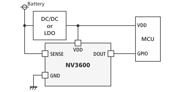
The NV3600 is using a CMOS based voltage detector. The high withstand voltage of 42 V at the SENSE pin allows this device to directly monitor battery voltage. NMOS open drain output type or CMOS output type can be selected for the output type. Therefore, external voltage divider resistors and pull-up resistors are no longer required, reducing the number of external components and the dark current of the system. In addition, the detection voltage and release voltage can be set separately, and the output logic at detection can also be selected to "Low" or "High". Therefore, the optimum operation can be realized according to the system.
Spec
| Standard | Industrial | Automotive | |
|---|---|---|---|
| Operating Voltage Range | 2.4 V to 6.0 V (7.0 V) SENSE pin: 0 V to 42.0 V (50.0 V) |
||
| Operating Temperature Range | -40°C to 105°C (125°C) | -40°C to 125°C (150°C) | -40°C to 125°C (150°C) |
| Supply Current | Typ. 1.4 µA (VDD pin only) Max. 4.0 µA (Includes SENSE pin current) |
||
| Detector Threshold Range | 3.3 V to 19.8 V (0.1 V step) | ||
| Detector Threshold Accuracy | ±0.6% (Ta = 25°C) ±1.5% (-40°C to 105°C) |
±0.6% (Ta = 25°C) ±1.5% (-40°C to 125°C) |
±0.6% (Ta = 25°C) ±1.5% (-40°C to 125°C) |
| Release Voltage Range | 4.5 V to 22.2 V (0.1 V step) | ||
| Release Voltage Accuracy | ±0.6% (Ta = 25°C) ±1.5% (-40°C to 105°C) |
±0.6% (Ta = 25°C) ±1.5% (-40°C to 125°C) |
±0.6% (Ta = 25°C) ±1.5% (-40°C to 125°C) |
| Release Delay Time | Typ. 40 µs | ||
| Output Type | CMOS, Nch Open Drain | ||
| Package | SOT-23-5-DC | ||
Technical Documents
-
SPICE model download
You can download the product's SPICE model. Login/registration to myNISD is required to download.
-
NV3600 Typical Application


Quality & Packages
| Product Name | Compatibility | Package | Marking | Reliability |
|---|---|---|---|---|
| NV3600DCxxxxE1S |
|
SOT-23-5-DC | See datasheet | NV3600DCS |
| NV3600DCxxxxE1D |
|
SOT-23-5-DC | See datasheet | NV3600DCD |
| NV3600DCxxxxE1P |
|
SOT-23-5-DC | See datasheet | NV3600DCP |
| NV3600DCxxxxE1Q |
|
SOT-23-5-DC | See datasheet | NV3600DCQ |

- Refer to the datasheets for the details on the product.
- The package file or the datasheet includes package dimensions, taping specifications, taping reels dimensions, power dissipations, and recommended land pattern.
FAQ
Buy / Contact
-
Purchase, Request for samples and documentsSales are made through distributors. Please contact your local distributors for any sales-related inquiry such as price.
-
Available from 1 piece!Our electronic device products are available through our authorized online distributors.
-
Technical Support
NV3600 Series