


NJM8532 Series
14V, Low Noise, Low Power, Rail-to-Rail Input/Output, Operational Amplifier
- Download Datasheet
- Point
-
Provides at-a-glance product features, functions, and concepts.
- ECAD Model: Learn more
-


Description
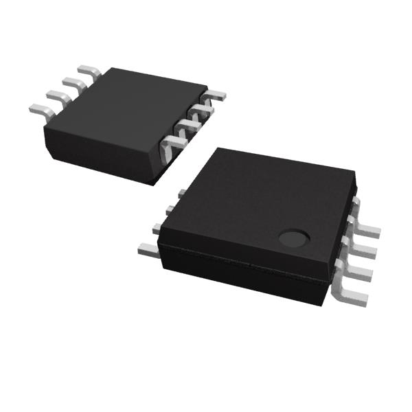
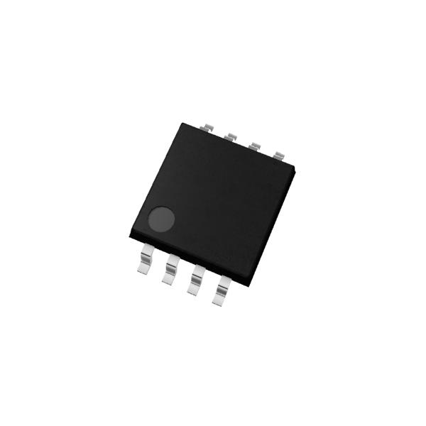
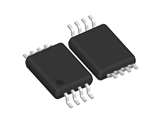
The NJM8530/NJM8532/NJM8534 are single/dual/quad rail to rail input and output single supply operational amplifier featuring 14V supply voltage, low noise and low power. A wide supply voltage range from 1.8V to 14V with a rail to rail input and output allows the device to be used in wide variety of applications, such as audio amplifier, hi-side current sensing, buffering and others. Furthermore, low supply current of 580µA typical at NJM8532 combined with a wide bandwidth of 1MHz and low very low noise of 10nV/√Hz at 1kHz make NJM8530/NJM8532/NJM8534 very suitable for a variety of battery-powered applications that require a good balance between low power, low noise and wide bandwidth. NJM8530/NJM8532/NJM8534 can drive up to approximately 1000pF, and is unity-gain stable. Operating temperature range is -40°C to 125°C. The NJM8530(single) is available in 5-pin SOT-23 package. NJM8532(dual) is available in 8-pin DMP, SSOP and MSOP(TVSP): meet JEDEC MO-187-DA / thin type package. NJM8534(quad) is available in 14-pin SSOP package.
Applications
- Battery-powered instruments, Audio, Sensor applications, Medical, Security
- High-side/Low-side Current sensing amplifiers
- Active Filters
- Analog-to-digital / Digital-to-analog Buffers
- Handheld Test Equipment
- Handheld Test Equipment
Spec
| Standard | Automotive | |
|---|---|---|
| No.of Circuit | 2 ch. | |
| Power Supply | Single | |
| Supply Voltage | 1.8 V to 14 V | |
| Supply Current (Per ch.) | Typ. 0.29 mA to max. 0.45 mA | |
| Input Offset Voltage | Typ. 1 mV to max. 4 mV | Typ. - mV to max. 5 mV |
| Slew Rate | Typ. 0.4 V/μsec | |
| Input Bias Current | Typ. 50 nA to max. 250 nA | Typ. - nA to max. 275 nA |
| Input Offset Current | Typ. 5 nA to max. 100 nA | Typ. - nA to max. 100 nA |
| GBW | Typ. 1 MHz | |
| Noise Voltage (en) | Typ. 10 nV/√Hz | |
| Input Offset Drift | Typ. 1.5 μV/℃ | |
| Wide Operating Temperature | -40°C to 125°C | |
| Junction Temp. | 150°C | |
| Min Stable Gain | 1 V/V | |
| Package | MSOP8(MSOP8(TVSP8)) DMP8 SSOP8 |
MSOP8(VSP8) |
| AEC-Q100 | AEC-Q100 grade1 | |
| Note(1) | Capacitive Load Drive (1000pF) | |
Technical Documents
-
Design Support
-
SPICE model download
You can download the product's SPICE model. Login/registration to myNISD is required to download.


Quality & Packages
| Product Name | Compatibility | Package | Marking | Reliability |
|---|---|---|---|---|
| NJM8532V |
|
SSOP8 | - | NJM-1-s-fr |
| NJM8532M |
|
DMP8 | - | NJM-1-s-fr |
| NJM8532RB1 |
|
MSOP8(TVSP8) | - | NJM-1-s-fr |
| NJM8532R-Z |
|
MSOP8(VSP8) | - | - |
| NJM8532R-T1 |
|
MSOP8(VSP8) | - | NJM-1-s-fr |

- Refer to the datasheets for the details on the product.
- The package file or the datasheet includes package dimensions, taping specifications, taping reels dimensions, power dissipations, and recommended land pattern.
Qualification Test Plan (QTP) Sheets
To download the QTP sheets, a myNISD account is required. If you do not have an account, please register in advance.If you already have an account, please click the button below. After logging in to myNISD, the QTP sheet list page for the corresponding series will be displayed.
FAQ
Buy / Contact
-
Purchase, Request for samples and documentsSales are made through distributors. Please contact your local distributors for any sales-related inquiry such as price.
-
Available from 1 piece!Our electronic device products are available through our authorized online distributors.
-
Technical Support