


RP107 Series
Output Capacitor-less 200mA LDO Regulator
RP107 Series
Output Capacitor-less 200mA LDO Regulator


拡大
:q
:q
Description
The RP107 Series are CMOS-based LDO regulators featuring 200 mA output. Since the output capacitor and noise bypass capacitor are able to be reduced and the packages are small DFN(PL)1212-6 and SC-88A, high density mounting on boards are possible. The input voltage (VIN) is as low as Min.1.4 V and the output voltage can be set from 1.0 V. Supply current is as low as 9.5µA compared to existing lines. The CE pin can switch the regulator to standby mode.
Spec
| Standard | |
|---|---|
| Input Voltage Range | 1.4 V to 5.25 V (6.0 V) |
| Operating Temperature Range | -40°C to 85°C (125°C) |
| Supply Current | Typ. 9.5 µA |
| Standby Current | Typ. 0.1 µA |
| Output Voltage Range | 1.0 V to 4.2 V (0.1 V step) |
| Output Voltage Accuracy | ±1.0% (Ta = 25°C) |
| Output Voltage Temperature Coefficient | Typ. ±100 ppm/°C |
| Line Regulation | Typ. 0.02%/V |
| Output Current | 200 mA |
| Ripple Rejection | Typ. 70 dB (f = 1 kHz, VOUT ≥ 1.2 V) Typ. 65 dB (f = 1 kHz, 1.2 V < VOUT < 2.2 V) Typ. 60 dB (f = 1 kHz, VOUT ≥ 2.2 V) |
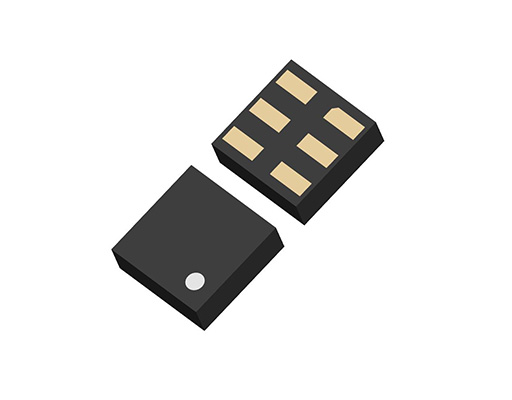
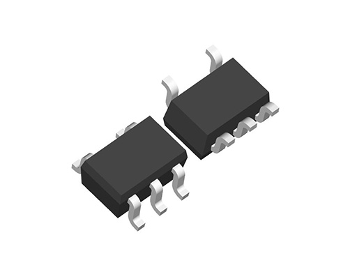
| Package | DFN(PL)1212-6, SC-88A |
Protections / Functions
| TSD | Reverse | Current Limit | ISC | Inrush | ECO mode | Auto Discharge | External Driver | PGOOD | Soft Start |
|---|---|---|---|---|---|---|---|---|---|
 |
|
|
|
Functional Description
| TSD | Thermal Shutdown Function |
|---|---|
| Reverse Current Protection | Reverse Current Protection |
| Current Limit | Overcurrent Protection |
| ISC | Short Current Protection |
| Inrush Current Limit | Inrush Current Protection |
| ECO mode | ECO Function |
| Auto Discharge | Auto Discharge Function |
| External Driver | External Output Driver Transistor |
| PGOOD | Power-Good |
| Soft Start | Soft Start Function |
Technical Documents
-
Typical Application
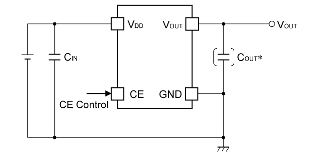
CIN: 0.1µF
*) The RP107 Series are using an output capacitor as phase compensation to ensure a stable operation even if the output load fluctuates. To reduce the output voltage fluctuation, it is imperative that a 0.1µF to 10µF output capacitor be used. -
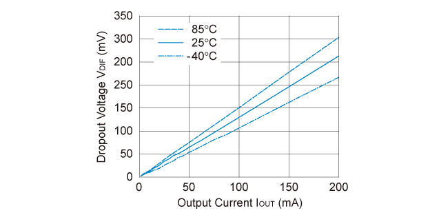
RP107x30xx Dropout Voltage vs. Output Current
Quality & Packages

- Refer to the datasheets for the details on the product.
- The package file or the datasheet includes package dimensions, taping specifications, taping reels dimensions, power dissipations, and recommended land pattern.
FAQ
Buy / Contact
-
Purchase, Request for samples and documentsSales are made through distributors. Please contact your local distributors for any sales-related inquiry such as price.
-
Available from 1 piece!Our electronic device products are available through our authorized online distributors.
-
Technical Support
RP107 Series