







Wafer Foundry—Kawagoe Plant
As a leading foundry manufacturer for analog and mixed-signal products, Nisshinbo Micro Devices Inc. offers highly reliable process technologies, which are well optimized in our own product development.
The technologies are ranging from 4.0 to 0.35µm, and Bipolar, CMOS with HVMOS, high speed BiCMOS, and BCD. Since the technologies are available on 5", and 8" wafers, Nisshinbo Micro Devices can appropriately respond to wide range production volume with our two manufacturing fab and UMC' 8" fab.
Process
| Process | Details | |
|---|---|---|
| Complimentary 40V High Speed Bipolar with TFR Application : OpAmp |
126KB | 2.0µm rule NPN ft= 2.9GHz, Vertical PNP ft= 3.7GHz Wafer Size 5" |
| High Speed BiCMOS Application : Industrial, Visual, Sensor AFE |
217KB | 0.8μm rule Bipolar 10V NPN ft= 8.0GHz, Vertical PNP ft= 5.5GHz, CMOS 5V Wafer Size 5" |
| Analog CMOS+HV Application : Power Supply, Audio, OpAmp |
212KB | 0.7µm rule LV 5V, HV 20V/30V/36V Wafer Size 5" |
| BCD Application : Power Supply, OpAmp |
Please contact us. | 0.35µm rule Bipolar 15V NPN, LPNP, CMOS 3.3V/5.0V, DMOS 40V/50V Wafer Size 8"(*1) |
| Analog CMOS+HV Application : Power Supply, OpAmp |
Please contact us. | 0.35µm rule LV 3.3V, MV 5.0V, HV 12~36V Wafer Size 8"(*1) |
(*1) :This process was developed in cooperation with UMC.
Inspection Items on Foundry Service
- Process control monitor (Device characteristics)
- Appearance defects
Optional Services
- Wafer sort
- Final Test
- Package
Product Forms
The PCM data is attached to the product at delivery.
- Wafer
- Bare die
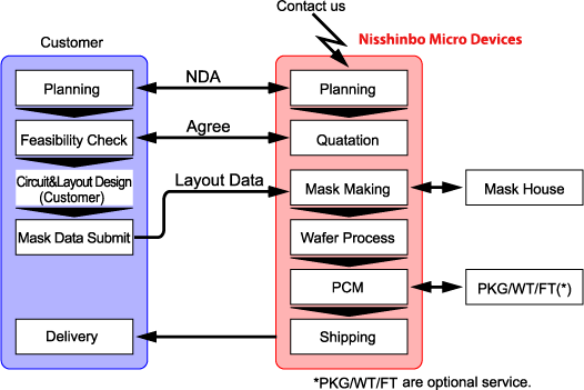
Business Flow
The standard business flow of foundry service is as follows. If you have any questions, please contuct us.
Contact Us
For inquiries about our foundry services, please use this form. A representative will contact you.
-
Foundry Services
