


NJW4191 Series
Inverting Charge Pump IC
NJW4191 Series
Inverting Charge Pump IC


拡大
:q
:q
Description
The NJW4191 is an inverting charge pump IC that operates wide 4.7V to 17V input range. With only the external part of an input/output capacitor and a charge pump capacitor, it can compose the inverting voltage circuit. It has a high current capability and a corresponding to small-sized capacitor compared with conventional product such as popular 7660/7662. For usability, it has ON/OFF function, Output Voltage Adjustable function and external synchronous function. The NJW4191 is suitable for the bias voltage of liquid crystal panels, CCD, sensors and operational amplifiers. There is the NJW4190 for doubler voltage output application.
Spec
| Standard | |
|---|---|
| Operating Current | Max. 1.22 mA |
| Operating voltage range | 4.7V to 17V |
| Output Resistance | Max. 34 Ω |
| Structure | Bi-CMOS Technology |
| Wide Operating Temperature | -40℃ to +85℃ |
| Junction Temp. | +150℃ |
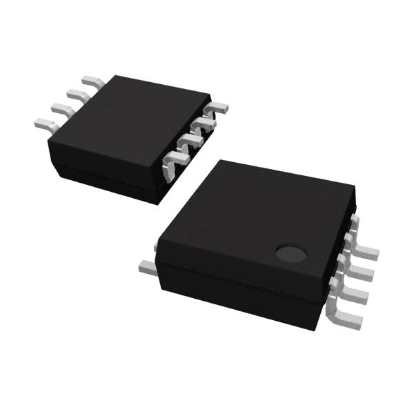
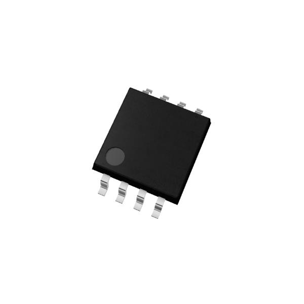
| Package | MSOP8(VSP8),DMP8 |
| Inverted Output | Max. -17V |
| Maximum Output Current | Max. 55mA |
| Built-in Oscillation Circuit | Typ. 300kHz |
| External Synchronization Function | divide-by-4 counter(A ver.) |
| Note | Correspond to Ceramic Capacitor(MLCC) VOUT Programmable ON/OFF Function Thermal Shutdown |
| Note(2) | Function Compatible to NJU7660/NJU7662 Doubler Circuit (The NJW4190 is not pin compatible to NJU7660/62.) |
Technical Documents
-
Evaluation Board

Quality & Packages
| Product Name | Compatibility | Package | Marking | Reliability |
|---|---|---|---|---|
| NJW4191R |
|
MSOP8(VSP8) | - | NJW-1-s-fr |
| NJW4191M |
|
DMP8 | - | NJW-1-s-fr |

- Refer to the datasheets for the details on the product.
- The package file or the datasheet includes package dimensions, taping specifications, taping reels dimensions, power dissipations, and recommended land pattern.
Buy / Contact
-
Purchase, Request for samples and documentsSales are made through distributors. Please contact your local distributors for any sales-related inquiry such as price.
-
Available from 1 piece!Our electronic device products are available through our authorized online distributors.
-
Technical Support
NJW4191 Series