


RP300 Series
0.8% Accuracy Voltage Detector with Delay Function (Internal Counter Type)


Description
The RP300 Series are CMOS-based voltage detector ICs with the built-in output delay circuit. There is no hysteresis between the detector threshold and the released voltage. By inputting "L" signal to MR pin, the manual reset signal is outputted. A delay capacitor is not needed, because the output delay time of 50 ms or 200 ms is generated with the counter in the IC. Additionally, the high accuracy output delay time at ±5% allows easy control of the start-up sequence. In addition to SOT-23-5 packages, a 1mm square DFN(PL)1010-4B package is also available.
Spec
| Standard | |
|---|---|
| Operating Voltage Range | 0.72 V to 5.50 V (6.0 V) |
| Operating Temperature Range | -40°C to 85°C (125°C) |
| Supply Current | Typ. 0.95 µA (−VSET = 3.08 V, VDD = 3.18 V) |
| Detector Threshold Range | 1.1 V, 2.32 V, 2.63 V, 2.7 V, 2.8 V, 2.93 V, 3.08 V, 4.2 V, 4.38 V, 4.6 V |
| Detector Threshold Accuracy | ±0.8% (1.7 V ≤ -VSET), ±1.0% (-VSET < 1.7 V) |
| Detector Threshold Temperature Coefficient | Typ. ±50 ppm/°C |
| Release Delay Time | Typ. 50 ms, 200 ms |
| Release Delay Time Accuracy | ±5% (25°C), ±15% (−40°C ≤ Ta ≤ 85°C) |
| Output Type | CMOS, Nch Open Drain |
| Package | DFN(PL)1010-4B, SOT-23-5 |
Technical Documents
-
SPICE model download
You can download the product's SPICE model. Login/registration to myNISD is required to download.
-
RP300xxxxA Timing Chart
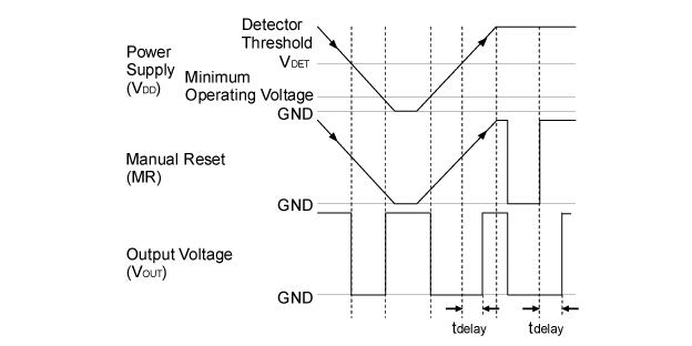
The detector threshold is the same as the released voltage, not hysteresis.
-
RP300xxxxC Timing Chart
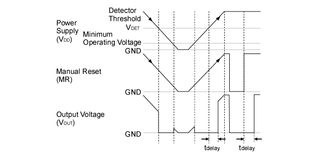
The detector threshold is the same as the released voltage, not hysteresis.


Quality & Packages
| Product Name | Compatibility | Package | Marking | Reliability |
|---|---|---|---|---|
| RP300Kxxxx-TR |
|
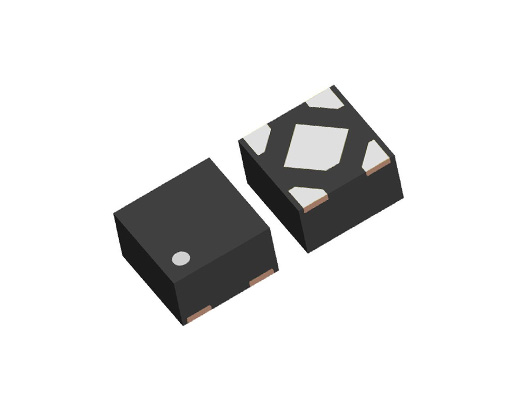
DFN(PL)1010-4B | See datasheet | RP300K |
| RP300Nxxxx-TR-FE |
|
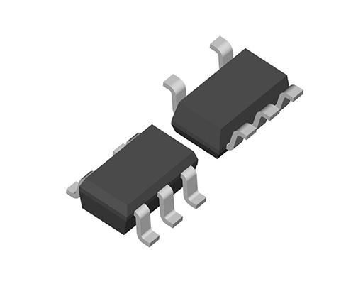
SOT-23-5 | See datasheet | RP300N-FE |

- Refer to the datasheets for the details on the product.
- The package file or the datasheet includes package dimensions, taping specifications, taping reels dimensions, power dissipations, and recommended land pattern.
FAQ
Buy / Contact
-
Purchase, Request for samples and documentsSales are made through distributors. Please contact your local distributors for any sales-related inquiry such as price.
-
Available from 1 piece!Our electronic device products are available through our authorized online distributors.
-
Technical Support