


RP111 Series
Low Voltage Good Load Transient Response 500mA LDO Regulator


Description
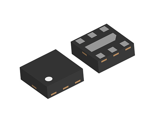
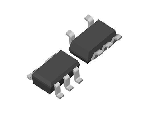
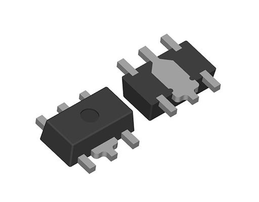
The RP111 Series are CMOS-based LDO regulators featuring 500mA output current. The minimum input voltage is as low as 1.4V and the output voltage can be set from 0.7V. Due to a built-in 0.46Ω (at VSET=2.8V) on-resistor, RP111 can provide a low dropout voltage. RP111 also features a ripple rejection at 75dB and low noise. The output voltage accuracy is as high as ±0.8%. The accuracy of output voltage of RP111 including the temperature characteristics and the load transient response has been improved. The Typ. and Max. value of under/overshoot accordnig to the various output current are shown in the typical characteristics in the datasheet, therefore the accuracy of the output voltage estimation will be easy on the actual operating cases. In addition to a fold-back protection circuit built into conventional regulators, RP111 contains a thermal shutdown circuit and an inrush current limit circuit. RP111 is offered in 5-pin SOT-23-5 and 5-pin SOT-89-5 packages. It is also offered in a 6-pin DFN1212-6 package, 1.2 mm x 1.2 mm, for consumer and industrial applications and a 6-pin HSOP-6J package for automotive application.
Spec
| Standard | Industrial | Automotive | |
|---|---|---|---|
| Input Voltage Range | 1.4 V to 5.25 V (6.0 V) | ||
| Operating Temperature Range | -40°C to 85°C (125°C) | -40°C to 105°C (125°C) | -40°C to 105°C (150°C) |
| Supply Current | Typ. 80 µA | ||
| Standby Current | Typ. 0.1 µA | ||
| Output Voltage Range | 0.7 V to 3.6 V (0.1 V step) | Internally Fixed Ver.: 0.7 V, 1.2 V, 1.5 V, 1.8 V, 2.5 V, 2.7 V, 2.8 V, 3.0 V, 3.3 V, 3.4 V Externally Adjustable Ver.: 0.7 V to 3.6 V with external resistors |
Internally Fixed Ver.: 0.7 V, 1.1 V, 1.2 V, 1.5 V, 1.8 V, 2.5 V, 2.8 V, 2.85 V, 2.9 V, 3.0 V, 3.3 V, 3.4 V Externally Adjustable Ver.: 0.7 V to 3.6 V with external resistors |
| Output Voltage Accuracy | ±0.8% (Ta = 25°C, VSET ≥ 1.8 V) | ||
| Output Voltage Temperature Coefficient | Typ. ±30 ppm/°C (VSET ≥ 1.8 V) | ||
| Dropout Voltage | Typ. 0.23 V (IOUT = 500 mA, VSET = 2.5 V) | ||
| Line Regulation | Typ. 0.02%/V | ||
| Output Current | 500 mA | ||
| Ripple Rejection | Typ. 75 dB (f = 1 kHz) Typ. 70 dB (f = 10 kHz) |
||
| Package | DFN1212-6, SOT-23-5, SOT-89-5 | DFN1212-6, SOT-23-5, SOT-89-5 | SOT-23-5, SOT-89-5, HSOP-6J |
| 入力過渡応答 | Typ. ±1.5 mV (VIN: VSET + 0.5 V ⇔ VSET + 1.5 V (tr = tf = 5.0 µs), VIN ≥ 1.4 V, IOUT = 30 mA) | ||
Protections / Functions
| TSD | Reverse | Current Limit | ISC | Inrush | ECO mode | Auto Discharge | External Driver | PGOOD | Soft Start |
|---|---|---|---|---|---|---|---|---|---|
 |
|
|
|
|
Functional Description
| TSD | Thermal Shutdown Function |
|---|---|
| Reverse Current Protection | Reverse Current Protection |
| Current Limit | Overcurrent Protection |
| ISC | Short Current Protection |
| Inrush Current Limit | Inrush Current Protection |
| ECO mode | ECO Function |
| Auto Discharge | Auto Discharge Function |
| External Driver | External Output Driver Transistor |
| PGOOD | Power-Good |
| Soft Start | Soft Start Function |
Technical Documents
-
Partner Board Qualifications (Lattice Semiconductor)
Nisshinbo Micro Devices parts are officially registered in reference design of Lattice FPGA system.
SPICE model download
You can download the product's SPICE model. Login/registration to myNISD is required to download.
-
Typical Application: Externally adjustable output voltage type
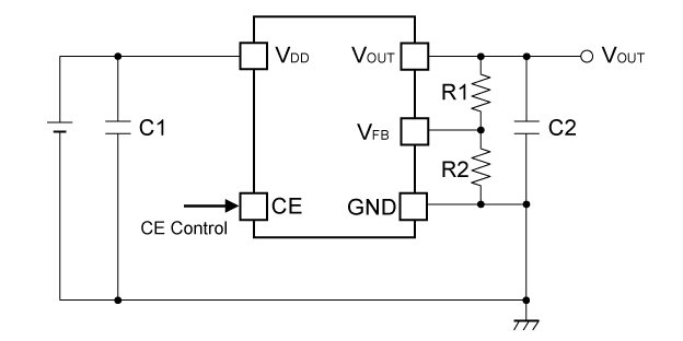
CIN: 1.0 µF, COUT: 4.7 µF
-
Typical Application: Internally fixed output voltage type
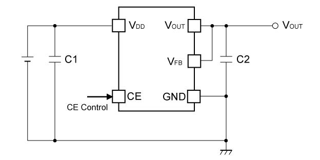
CIN,COUT: 1.0 µF
-
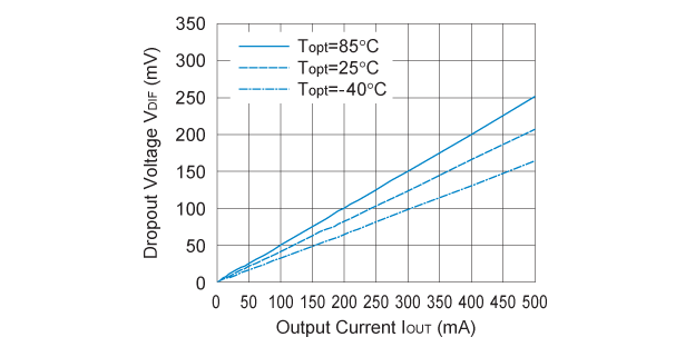
RP111x281x Dropout Voltage vs. Output Current


Quality & Packages
| Product Name | Compatibility | Package | Marking | Reliability |
|---|---|---|---|---|
| RP111Lxx1x-TR |
|
DFN1212-6 | RP111L | RP111L |
| RP111Nxx1x-TR-FE |
|
SOT-23-5 | RP111N | RP111N-FE |
| RP111Hxx1x-T1-FE |
|
SOT-89-5 | RP111H | RP111H-FE |
| RP111Lxx1x-TR-Y |
|
DFN1212-6 | RP111L | RP111L-Y |
| RP111Nxx1x-TR-YE |
|
SOT-23-5 | RP111N | RP111N-YE |
| RP111Hxx1x-T1-YE |
|
SOT-89-5 | RP111H | RP111H-YE |
| RP111Nxx1x-TR-JE |
|
SOT-23-5 | RP111N | RP111N-JE |
| RP111Nxx1x-TR-AE |
|
SOT-23-5 | RP111N | RP111N-AE |
| RP111Hxx1x-T1-JE |
|
SOT-89-5 | RP111H | RP111H-JE |
| RP111Hxx1x-T1-AE |
|
SOT-89-5 | RP111H | RP111H-AE |
| RP111Sxx1x-E2-JE |
|
HSOP-6J | RP111S | RP111S-JE |
| RP111Sxx1x-E2-AE |
|
HSOP-6J | RP111S | RP111S-AE |

- Refer to the datasheets for the details on the product.
- The package file or the datasheet includes package dimensions, taping specifications, taping reels dimensions, power dissipations, and recommended land pattern.
Qualification Test Plan (QTP) Sheets
To download the QTP sheets, a myNISD account is required. If you do not have an account, please register in advance.If you already have an account, please click the button below. After logging in to myNISD, the QTP sheet list page for the corresponding series will be displayed.
FAQ
Buy / Contact
-
Purchase, Request for samples and documentsSales are made through distributors. Please contact your local distributors for any sales-related inquiry such as price.
-
Available from 1 piece!Our electronic device products are available through our authorized online distributors.
-
Technical Support