


NR1620 Series
150mA 0.4V Output & Ultra-Low Supply Current Voltage Regulator
NR1620 Series
150mA 0.4V Output & Ultra-Low Supply Current Voltage Regulator
- Download Datasheet
- Point
-
Provides at-a-glance product features, functions, and concepts.
- ECAD Model: Learn more
-


拡大
:q
:q
Description
The NR1620 series are a voltage regulator manufactured using a CMOS process with the output current of 150 mA. This device supports the VIN input voltage as low as 0.6 V and the output voltage as low as 0.4 V. This device can be used as a power supply for the core of a microcontroller, various interfaces, etc. In addition, the ultra-low quiescent current of 0.4 μA makes it suitable to use in systems that require low consumption and long time operation, such as battery-driven systems. NMOS power transistors are driven by a bias power input pin (VBIAS) independent of the power input pin (VIN) to achieve highly efficient regulation.
Spec
| Standard | |
|---|---|
| Input Voltage Range | VBIAS : 2.4 V to 5.5 V (6.5 V) VIN : 0.6 V to VBIAS (6.5 V) |
| Operating Temperature Range | -40°C to 85°C (125°C) |
| Supply Current | Typ. 0.4 µA |
| Standby Current | Typ. 4 nA |
| Output Voltage Range | 0.4 V to 1.2 V (0.1 V step) |
| Output Voltage Accuracy | Ta = 25°C : ±9.9 mV (0.4 V ≤ VSET ≤ 0.9 V), ±1.1% (0.9 V < VSET ≤ 1.2 V) -40°C ≤ Ta ≤ 85°C : ±18 mV (0.4 V ≤ VSET ≤ 0.9 V), ±2.0% (0.9 V < VSET ≤ 1.2 V) |
| Dropout Voltage | Typ. 150 mV (IOUT = 150 mA, VSET = 1.0 V, VBIAS = 2.4 V) |
| Ripple Rejection | Typ. 90 dB (f = 1 kHz, Ripple in VIN) Typ. 60 dB (f = 100 kHz, Ripple in VIN) |
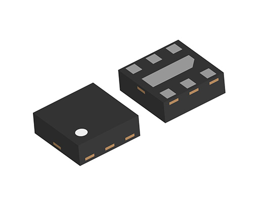
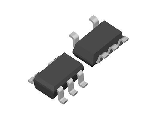
| Package | DFN1212-6-GK, SOT-23-5-DC |
Protections / Functions
| TSD | Reverse | Current Limit | ISC | Inrush | ECO mode | Auto Discharge | External Driver | PGOOD | Soft Start |
|---|---|---|---|---|---|---|---|---|---|
 |
|
|
|
|
Functional Description
| TSD | Thermal Shutdown Function |
|---|---|
| Reverse Current Protection | Reverse Current Protection |
| Current Limit | Overcurrent Protection |
| ISC | Short Current Protection |
| Inrush Current Limit | Inrush Current Protection |
| ECO mode | ECO Function |
| Auto Discharge | Auto Discharge Function |
| External Driver | External Output Driver Transistor |
| PGOOD | Power-Good |
| Soft Start | Soft Start Function |
Technical Documents
-
SPICE model download
You can download the product's SPICE model. Login/registration to myNISD is required to download.
-
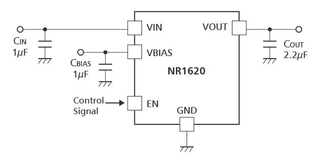
Typical Application Circuit
-
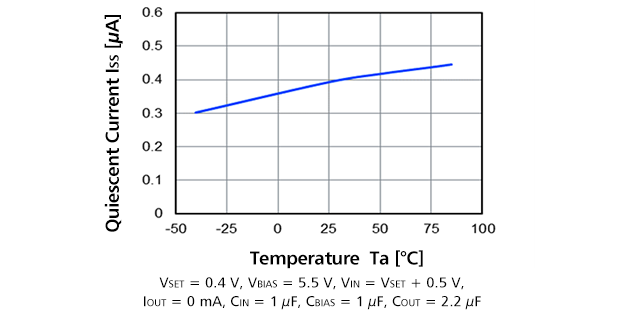
Quiescent Current


Quality & Packages
| Product Name | Compatibility | Package | Marking | Reliability |
|---|---|---|---|---|
| NR1620GKxxxxE4S |
|
DFN1212-6-GK | See datasheet | NR1620GKS |
| NR1620DCxxxxE1S |
|
SOT-23-5-DC | See datasheet | NR1620DCS |

- Refer to the datasheets for the details on the product.
- The package file or the datasheet includes package dimensions, taping specifications, taping reels dimensions, power dissipations, and recommended land pattern.
FAQ
Buy / Contact
-
Purchase, Request for samples and documentsSales are made through distributors. Please contact your local distributors for any sales-related inquiry such as price.
-
Available from 1 piece!Our electronic device products are available through our authorized online distributors.
-
Technical Support
NR1620 Series