


For the RF devices, are there any precautions in using a multilayer board?
- * This FAQ mainly explains GaAs products using GaAs substrates and RF CMOS products using SOI technology.
RF Deviceboard
For RF lines (microstrip lines), please design the RF line width to have a characteristic impedance of 50 ohm (75 ohm for TV applications) based on the thickness and the relative permittivity of the dielectric.
And if the RF line is drawn on the outer layer and the DC line is drawn on the middle layer, please design the pattern so that these lines are not coupled each other.
When the distance from an RF line layer at the surface to a ground layer (thickness of dielectric) is greater than that of the evaluation board described in the datasheet, RF characteristics may be changed due to long distance to the ground.
Therefore, please pay attention to the following points when designing a multilayer board: RF line design; coupling between wires; and dielectric thickness.
-
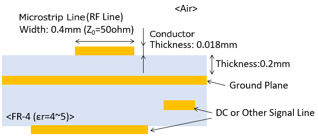
Example of RF Lines with 50-ohm Characteristic Impedance.