


Are there any precautions in designing printed circuit boards for RF devices?
- * This FAQ mainly explains GaAs products using GaAs substrates and RF CMOS products using SOI technology.
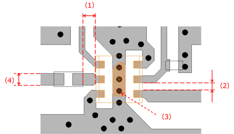
RF Deviceboard
Characteristics of high frequency products may be changed due to the space between the IC and external parts (please see (1) in the figure) and the space of RF lines (high frequency lines).
If the space between the DC and RF lines becomes close, the RF characteristics may change. (Please see (2) in the figure.)
Moreover, in case of the high power RF switches and the power amplifiers, a malfunction may occur.
The state of the ground may be negatively affected by too small diameter via holes or the via holes too distant from the IC, which may cause changes in RF characteristics.
From the reasons above, please design the pattern to be as same with our reference evaluation board shown in the datasheet (e.g. RF lines, DC lines, the space of external parts, the location and size of vias, and so on) as possible.
Also, please design the pattern of RF lines to have a characteristic impedance of 50 Ω. (Please see (4) in the figure.)
-
Printed Circuit Board (PCB) Layout Precautions