


R5326 Series
Low Voltage Automatic ECO Mode Shift Dual 150mA Voltage Regulator


Description
The R5326 Series are CMOS-based auto mode switching dual LDO regulators featuring 150mA output. In auto switching mode, the operation can switch automatically to a fast response mode or a low power mode of the ECO function according to output current. (Automatic switching to fast response mode under IOUT > 3mA conditions or to low power mode under IOUT < 0.6mA conditions.) In low power mode, supply current is as low as 5.5µA. In fast response mode, ripple rejection is 70dB and noise is low. R5326 requires neither ECO pin for switching mode nor microcontroller pin. R5326 supports low voltage, featuring input voltage from 1.4V and output voltage from 0.8V. Standby mode and auto-discharge function are also available.
Spec
| Standard | |
|---|---|
| Input Voltage Range | 1.4 V to 6.0 V (6.5 V) |
| Operating Temperature Range | -40°C to 85°C (125°C) |
| Supply Current | Low Power Mode: Typ. 5.5 µA × 2 (VR1 & VR2) (IOUT = 0 mA) Fast Transient Mode: Typ. 50 µA × 2 (VR1 & VR2) (IOUT = 10 mA) |
| Standby Current | Typ. 0.1 µA (VR1 & VR2) |
| Output Voltage Range | 0.8 V to 4.2 V (0.1 V step) |
| Output Voltage Accuracy | ±1.0% (Ta = 25°C, VOUT > 1.5 V) |
| Output Voltage Temperature Coefficient | Typ. ±100 ppm/°C |
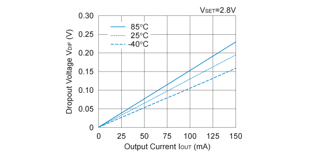
| Dropout Voltage | Typ. 0.19 V (IOUT = 150 mA, VOUT = 2.8 V) |
| Line Regulation | Typ. 0.02%/V |
| Output Current | 150 mA |
| Ripple Rejection | Typ. 70 dB (f = 1 kHz) Typ. 60 dB (f = 10 kHz) |
| Package | DFN(PL)1820-6 |
Protections / Functions
| TSD | Reverse | Current Limit | ISC | Inrush | ECO mode | Auto Discharge | External Driver | PGOOD | Soft Start |
|---|---|---|---|---|---|---|---|---|---|
 |
|
|
|
Functional Description
| TSD | Thermal Shutdown Function |
|---|---|
| Reverse Current Protection | Reverse Current Protection |
| Current Limit | Overcurrent Protection |
| ISC | Short Current Protection |
| Inrush Current Limit | Inrush Current Protection |
| ECO mode | ECO Function |
| Auto Discharge | Auto Discharge Function |
| External Driver | External Output Driver Transistor |
| PGOOD | Power-Good |
| Soft Start | Soft Start Function |
Technical Documents
-
Typical Application
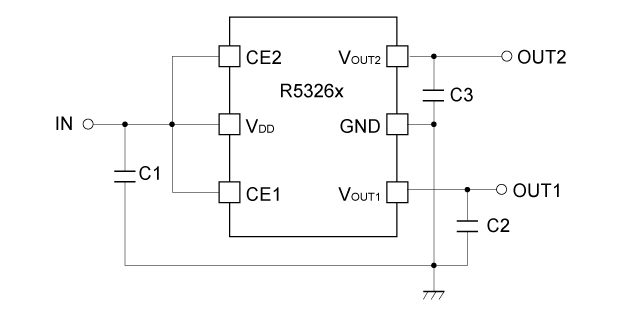
C1: 1.0 µF
C2, C3: 1.0 µF to 3.3 µF -
R5326K (VR1/VR2) Dropout Voltage vs. Output Current
Quality & Packages
| Product Name | Compatibility | Package | Marking | Reliability |
|---|---|---|---|---|
| R5326Kxxxx-TR |
|
DFN(PL)1820-6 | R5326K | R5326K |

- Refer to the datasheets for the details on the product.
- The package file or the datasheet includes package dimensions, taping specifications, taping reels dimensions, power dissipations, and recommended land pattern.
FAQ
Buy / Contact
-
Purchase, Request for samples and documentsSales are made through distributors. Please contact your local distributors for any sales-related inquiry such as price.
-
Available from 1 piece!Our electronic device products are available through our authorized online distributors.
-
Technical Support