


Ideal for Applications with Long Sleep Periods,
New Release of the NC4650 Series, a Boost Switching Regulator
- Industry-Leading Ultra-Low Quiescent Current of Iq = 70 nA Achieves High Efficiency at Light Loads -
New Release of the NC4650 Series, a Boost Switching Regulator
- Industry-Leading Ultra-Low Quiescent Current of Iq = 70 nA Achieves High Efficiency at Light Loads -
Nisshinbo Micro Devices Inc. released the NC4650 series, a boost switching regulator for use in consumer applications.
Advances in IoT technology and market expansion have led to an increase in the number of devices with data communication capabilities. In particular, many small IoT devices, security devices, and sensors for industrial equipment are powered by primary batteries, and low power consumption is required to extend battery life. Especially, power consumption during sleep mode has become an issue. In addition, noise reduction is required to prevent transmission errors during data communication.
This product achieves an ultra-low quiescent current of Iq = 70 nA (reduced to 1/4 of our conventional product) and contributes to longer battery life and equipment operation through highly efficient power conversion in sleep mode. It also features a "low ripple mode" for noise reduction, which can be easily switched via the MODE pin. The low ripple and excellent load transient response characteristics suppress transmission errors during data communication. In addition, the PWM/PFM auto-switching control method is used to achieve efficient power supply by automatically switching to PFM when the load current is low and to PWM when the load current becomes high.
The EN pin can be used to switch to the shutdown state with Iq = 50 nA. The operation at the shutdown state can be selected from the following three versions.
- VIN – VOUT Complete Disconnect: NC4650ZAxxxAE2S, NC4650ZAxxxCE2S
- VOUT Discharge (Auto Discharge Function): NC4650ZAxxxBE2S
- VIN – VOUT Pass-Through (Seamless Pass-Through Function): NC4650ZAxxxDE2S
The product uses the ultra-small WLCSP-6-ZA1 package (1.3 × 0.92 × 0.4 mm), which is suitable for high-density mounting.
| Product Name | NC4650 Series |
| Sample Unit Price (Reference unit price when purchasing 1000 units, tax Included*) |
JPY 330 |
| Sample Order Start Date | April 10, 2025 |
| Monthly Production | 1 million |
- *The price is based on the consumption tax rate as of April 2025.
Features
1. Switching between Low Quiescent Current Mode and Low Ripple Mode via MODE Pin
The product has the MODE pin to switch between normal mode with low quiescent current and low ripple mode depending on the operating conditions.
Normal mode achieves high efficiency power conversion (>90%) even at light loads thanks to very low quiescent current (at VIN = 3.0 V, VOUT = 3.3 V, IOUT = 0.01 mA).
Low ripple mode provides low ripple and improved load transient response, making it ideal for noise-sensitive systems.
Efficiency Characteristics (Normal Mode / Low Ripple Mode, VOUT = 3.3 V)

Ripple Characteristics (Normal Mode / Low Ripple Mode)

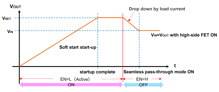
2. Seamless Pass-Through Function (NC4650ZAxxxDE2S)
The product offers a version that features seamless pass-through during the shutdown state.
The seamless pass-through function outputs the voltage of the VIN and SW pins as they are to the VOUT pin, while suppressing voltage fluctuations on the VOUT pin and reverse current to the SW pin during pass-through.
After the product is switched to the shutdown state by a “high” level control signal input to the EN pin, the output voltage drops due to the load. When the output voltage drops to the voltage of the VIN pin, the output voltage continues to be as the voltage of the VIN pin.
Applications
- Hearing Aids, Medical Patches
- Smartwatches
- IoT Edge Devices
- Keyless Entry Systems
- Alarms, Wireless Sensor Networks
Product Photo

NC4650 Series, WLCSP-6-ZA1 (1.3 × 0.92 × 0.4 mm)
Main Specifications (Please refer to the datasheet for details.)
| Item | NC4650 Series |
| Input Voltage Range | 0.6 V to 5.5 V (Absolute Maximum Rating: 6.5 V) |
| Output Voltage Range | 1.8 V to 5.0 V (0.1 V step) |
| Startup Voltage | Typ. 0.8 V |
| Quiescent Current | Typ. 70 nA / 90 µA (Normal Mode / Low Ripple Mode) |
| Switch Current Limit | Typ. 1 A / 0.65 A (VSET ≥ 2.5 V / VSET < 2.5 V) |
| Operating and Junction Temperature Range | Ta = -40°C to 85°C Tj = -40°C to 125°C |
| Package | WLCSP-6-ZA1 (1.3 × 0.92 × 0.4 mm) |
Contact
-
Nisshinbo Micro Devices Inc.
