


Under Development: RN5T5611 Series, 3-channel Power Management IC Corresponding to Functional Safety
- For Automotive CMOS Image Sensors, Compliant with ISO26262 ASIL-D -
- For Automotive CMOS Image Sensors, Compliant with ISO26262 ASIL-D -
Nisshinbo Micro Devices Inc. announces that we are developing the RN5T5611 series, a power management multi-channel IC for automotive sensing cameras. It will be our first product compliant to the development process ISO26262 ASIL-D.
Overview
It is getting more important for today’s advancing automobiles to meet higher levels of “functional safety,” a design concept to clarify risks against failures and secure an acceptable level of safety even in case of failure. Especially, peripheral circuits for camera systems used in autonomous driving are required to meet high levels of functional safety.
The RN5T5611 series is a power management multi-channel IC for CMOS image sensors, which is compliant with the development process of ISO26262 ASIL-D. It includes two DC/DC switching regulators, one ultra-low noise LDO regulator, four monitoring circuits for over- and under-voltages, and a BIST function. The input voltage range is from 3.0 V to 5.5 V with a rating of 6.5 V, and the output voltage is flexibly settable by laser trimming. Also, the built-in I2C interface enables reading the status and partially changing settings of RN5T5611 series.
The RN5T5611 series adopts QFN0505-32-P7 (5.0 mm x 5.0 mm) as its package, featuring leadless wettable flank structure that makes it easy to conduct mounting inspection.
The RN5T5611 series is manufactured in our Yashiro Plant (Kato City, Hyogo Prefecture). The IC will be applicable to our Product Longevity Program that maintains product supply for 10 years in order to let customers use it for a long period without any concern on end of life (EOL). The sample order starting date is scheduled at the end of February 2022.
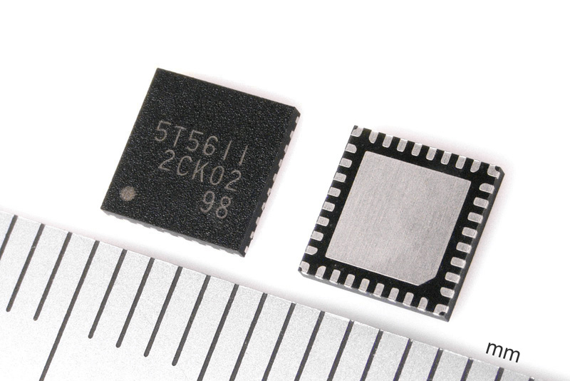
RN5T5611 series (QFN0505-32-P7 package)
| Product Name | RN5T5611 Series |
| Sample Price (per 1,000pieces) | JPY 770 (Tax included) |
| Sample Order Start Date | End of Feb 2022 |
| Monthly Production | 2 Million |
Features
1. Our First Product Compliant with ISO26262 ASIL-D
The RN5T5611 series is our first product manufactured through the development process compliant with ISO26262 ASIL-D. We adopt a development flow where we assign a person responsible for functional safety and take care of systematic faults. We also prepare a safety manual. These measures contribute to releasing customers from safety analysis on this product and reducing developing time.
Safety mechanisms include detection functions for over- and/or under-voltage, a diagnostic function to detect potential damage in safety mechanisms themselves, etc. For more information, please contact our sales team.
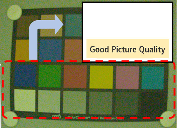
2. Built-in Ultra-low Noise and High PSRR LDO Regulator to Maximize Performance of CMOS Image Sensor
Fluctuations in the power supply to a CMOS image sensor caused by noise affects picture quality. Especially, countermeasures against noise are necessary for analog power supply to maximize the performance of CMOS image sensors. The LDO regulator included in the RN5T5611 series achieves ultra-low output noise of 6 μVrms and high power supply ripple rejection (PSRR) of 80 dB (f = 1 kHz) / 60 dB (f = 100 kHz) and is able to enhance the performance of CMOS image sensors without special measures.
-
RN5T5611
-
Competitor's LDO
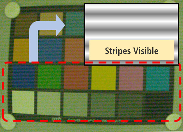
Comparison of picture quality with noise superimposed on the input to CMOS image sensor
3. Leadless Wettable Flank Package
The RN5T5611 adopts QFN0505-32-P7 package with safe pin layout considered. Although the package is leadless with the size of 5.0 mm x 5.0 mm, the wettable flank structure makes it easy to conduct visual inspection of solder joint.
Key Specifications
| Item | RN5T5611 Series |
| Input Voltage Range (VIN) | 3.0 V to 5.5 V (Maximum Rating 6.5 V) |
| DC/DC Output Voltage Range (VOUT1/2) | 1.0V to 3.3V ±1% (Max. 1.0 A) Fix voltage by lazer trimming at shipping |
| LDO Output Voltage Range (VOUT3) | 2.5 V to 3.5 V ±1% (Max. 200 mA) Fix voltage by lazer trimming at shipping |
| LDO Output Noise | Typ. 6 μVrms |
| LDO Ripple Rejection | Typ. 80 dB (f=1kHz) / Typ. 60 dB (f=100kHz) |
| UVP / OVP | 4 channels |
| Communication | I2C interface 1 MHz / 400 kHz |
| Functions | Thermal shutdown Auto discharge Analog and logic BIST Soft-start, short-circuit protection, UVLO, etc. |
| Package | 5.0 x 5.0 x 0.75 (mm) QFN0505-32-P7 |
News release in PDF format
Under Development: RN5T5611 Series, 3-channel Power Management IC Corresponding to Functional Safety
Contact
-
Nisshinbo Micro Devices Inc.
