


NJG1802K51
High Power SPDT Switch GaAs MMIC
NJG1802K51
High Power SPDT Switch GaAs MMIC


拡大
:q
Description
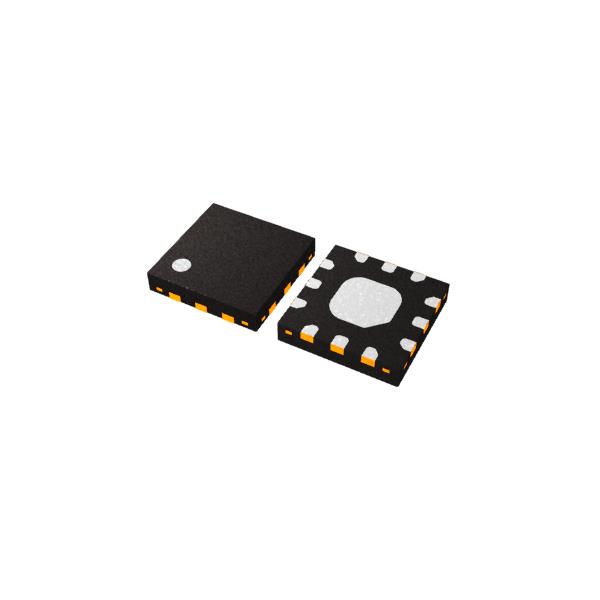
The NJG1802K51 is a GaAs SPDT switch MMIC suitable for LTE/UMTS/CDMA/GSM applications. The NJG1802K51 features very low insertion loss, high isolation and excellent linearity performance down to 1.8V control voltage at high frequency up to 2.7GHz. In addition, this switch is able to handle high power signals. For saving current consumption, the NJG1802K51 has a shutdown mode. The NJG1802K51 has ESD protection devices to achieve excellent ESD performances. No DC Blocking capacitors are required for all RF ports unless DC is biased externally. And the ultra small & ultra thin QFN12-51 package is adopted.
Applications
- LTE, UMTS, CDMA, GSM applications
- Post PA Switching, Antenna Switching and Bands Switching applications
- General Purpose Switching applications
Spec
| Standard | |
|---|---|
| Function | SPDT Switch |
| P-0.1dB | Typ. 36dBm |
| Power Level | High Power |
| Insertion Loss | 0.18dB/ 0.20dB/ 0.23dB typ. @f=0.9GHz/ 1.9GHz/ 2.7GHz |
| Frequency Range | 0.2GHz to 6GHz |
| Package Size | Typ. 2.0x2.0x0.375 mm |
| Low Control Voltage | VCTL(H)=1.8V typ. |
| Voltage Operation | VDD=2.7V typ. |
| Wide Operating Temperature | -40°C to 85°C |
| Junction Temp. | 150°C |
| Package | QFN12-51 |
| Low distortion | IIP3=+73dBm typ. @f=829+849MHz, PIN=24dBm IIP3=+73dBm typ. @f=1870+1910MHz, PIN=24dBm 2nd/3rd harmonics=-90dBc/ 90dBc typ. @f=0.9GHz, PIN=35dBm |
Technical Documents
Quality & Packages

- Refer to the datasheets for the details on the product.
- The package file or the datasheet includes package dimensions, taping specifications, taping reels dimensions, power dissipations, and recommended land pattern.
FAQ
Buy / Contact
-
Purchase, Request for samples and documentsSales are made through distributors. Please contact your local distributors for any sales-related inquiry such as price.
-
Available from 1 piece!Our electronic device products are available through our authorized online distributors.
-
Technical Support