


PMICs: Features and Benefits


01 Shortening development cycle times !
Flexible Sequence Control

- Sequence settings are adjustable to the platform and the power-supply structure of your applications.
- You can set a sleep-in/out sequence as well as a power on/off sequence.
The sequences of our PMICs are flexibly configurable by using one-time-programmable memory (OTP). An OTP is a kind of read-only memory which allows data to be registered only once. After data registration, the OTP becomes read-only. Here, in the premise of using an OTP to set a start-up sequence and default voltages, we will show you one example of a power-supply start-up timing chart and default values of each power supply.
Default voltages and start-up sequences are programmable with an OTP. These default settings can be changed by I2C access from the processor to the register. Also, you can select the interval of delay steps from 0.5 ms or 2 ms with an OTP. The steps cannot be changed with a register.
Example of Power-supply Start-up Timing Chart and Default Values of Each Power Supply
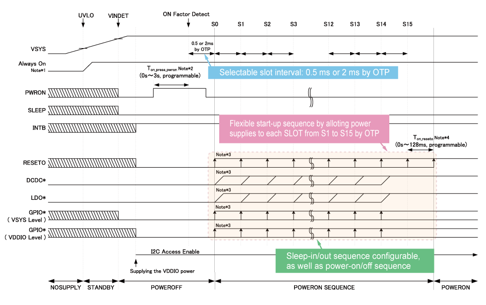

Sequence control is a function to control the power-on/off sequences at a system's starting up or turning to a sleep mode. The power-on order toward functional blocks inside an SoC is determined in advance, and a PMIC must control the power supplies to power the SoC according to the power-on order. This is one of the major purposes of sequence control. It prevents bus contention by powering on/off at a proper timing. Also, each power supply in a PMIC has various functions as a soft-start function and an inrush current prevention, and if all the power supplies turn on at the same time, the PMIC may malfunction due to its input voltage drop. Sequence control is also helpful to prevent malfunction by decentralizing the power-on timing of each power supply and by dispersing inrush current.
Flexible Voltage Setting according to Platform
Power-on sequences of our PMICs can be customized with an OTP flexibly according to the SoC system.
The OTP inside a PMIC has default setting data on a sequence and output voltage values at power-on according to customer requests or to the adopted SoC. These data are reflected on registers which set sequences or output voltages when the PMIC receives power.
- Default output voltages of a PMIC are settable with an OTP. You can change the default values by using a register subsequently.
- The wide settable output voltage range enables you to change these values according to your platform.
Default Voltage Table by Product
| RN5T567/8/9/10/12 | By Register | By OTP | |
|---|---|---|---|
| DCDC | 0.6V - 3.5V | 12.5mV Step | 50mV Step |
| LDO1-2 | 0.9V - 3.5V | 25mV Step | |
| LDO3 | 0.6V - 3.5V | ||
| LDO4 | 0.9V - 3.5V | ||
| LDO5 | 0.9V - 3.5V | ||
| LDORTC1 | 1.2V - 3.5V | ||
| LDORTC2 | 0.9V - 3.5V |
Multi-function GPIOs
for Flexible Configuration & Efficient Development
- Multi-function general purpose input/output pins (GPIOs) enable flexible input/output selections according to your application.
Selectable Functions of GPIOs
| Function | RN5T567/8/9/10/12 |
|---|---|
| PowerControl | On/Off/Reset |
| CLK32K | Out |
| LED Driver | ✓ |
| Enable_for_ext_IC | ✓ |
02 Reducing current consumption !
Modes-based Power Control
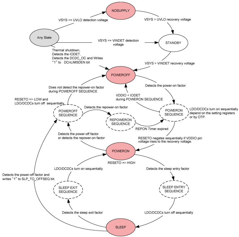
Our PMICs have various functions that contribute to reducing current consumption.
Modes-based Power Control
Our PMICs have various functions that contribute to reducing current consumption.
- The power control function can reduce current consumption by controlling the on/off state of each power supply with pins or registers according to the operating modes of a whole SoC.
A power control function can reduce current consumption by controlling on/off state of each power supply according to the SoC's operation (e.g. power-on, power-off, and sleep modes).
Regarding the sleep mode, it is possible to set which power supply to turn off, how much voltage the power supply outputs, and even the sequence of powering off by I2C easily.
* Click to enlarge
Power Control State Machine Diagram
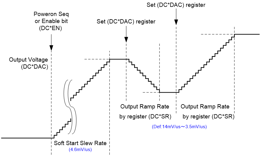
DVS(Dynamic Voltage Scaling)
DVS(Dynamic Voltage Scaling)
- A DVS function enables varible voltage control according to the status of a subsequent device. Even at operation it reduces current consumption of the logic circuits inside the device.
A DVS function dynamically changes power-supply voltages according to the operating mode of a subsequent device such as an SoC and an FPGA during supplying voltages to the device. This is one of methods to reduce current consumption during operation.Reducing regulators' voltages of a PMIC can reduce current consumption of logic circuits inside the subsequent device.Using this DVS function can reduce current consumption by reducing output voltages while maintaining power supply. The voltage transition is performed smoothly in steps in order to reduce ripples. This function is useful when the subsequent SoC or FPGA system requires less energy such as at a sleep mode or at a standby mode.
DVS Timing Chart
* Click to enlarge
03 Reducing Mounting Area !
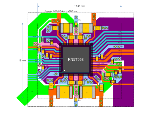
Power Management Functions in Single Chip
Power Management Functions in Single Chip
- Having multiple power management circuits and logic circuits in a single chip, a PMIC achieves smaller mounting area than the same number of voltage regulators.
- Using only one PMIC could reduce total cost, too.
| Product | Package Size | Mounting Size | Height |
|---|---|---|---|
| RN5T567 | 36mm2 | 191mm2 | 0.9mm |
| RN5T568/10/12 | 49mm2 | 279mm2 | 0.9mm |
| RN5T569 | 49mm2 | 279mm2 | 0.9mm |
Please feel free to contact us.