


RP124 Series
Low Supply Current 100mA LDO Regulator with Battery Monitor
RP124 Series
Low Supply Current 100mA LDO Regulator with Battery Monitor
- Download Datasheet
- Point
-
Provides at-a-glance product features, functions, and concepts.
- ECAD Model: Learn more
-


拡大
:q
:q
Description
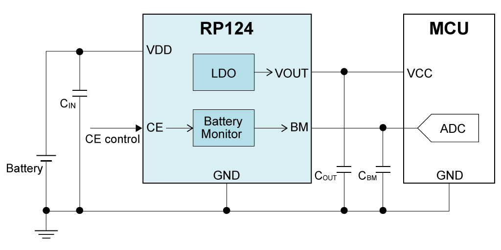
The RP124 is an LDO regulator with a battery monitor (BM) featuring ultra-low supply current. The battery monitor has a function which divides the input voltage (VIN) into 1/3 or 1/4. The battery charge remaining can be monitored by MCU. The buffering output enables directly inputting a signal into the low voltage A/D converter (ADC) with built-in MCU.
Key Benefits
- Achieving Low Supply Current of 0.3 µA, Longer Battery Life and Downsizing
- Requiring Only Three External Capacitors and Suitable for Space-saving Mounting for the Smaller Packages
Spec
| Standard | |
|---|---|
| Input Voltage Range | 1.7 V to 5.5 V (6.5 V) |
| Operating Temperature Range | -40°C to 85°C (125°C) |
| Supply Current | Typ. 0.3 µA (LDO Section) |
| Output Voltage Range | 1.2 V, 1.5 V, 1.8 V, 2.1 V, 2.2 V, 2.3 V, 2.4 V, 2.5 V, 2.7 V, 2.8 V, 3.0 V, 3.1 V, 3.3 V, 3.6 V |
| Output Voltage Accuracy | ±0.8% (Ta = 25°C) |
| Output Current | 100 mA |
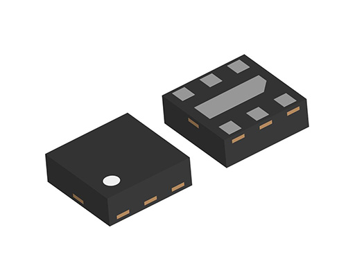
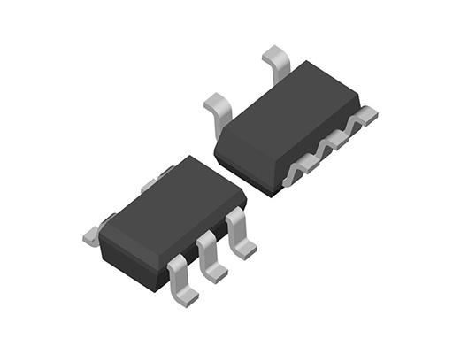
| Package | DFN1212-6, SOT-23-5 |
| BM Output Voltage | VIN/3 (RP124xxx3x) VIN/4 (RP124xxx4x) |
| BM Output Voltage Accuracy | ±20 mV |
| BM Output Current | Typ. 0.1 µA |
Protections / Functions
| TSD | Reverse | Current Limit | ISC | Inrush | ECO mode | Auto Discharge | External Driver | PGOOD | Soft Start |
|---|---|---|---|---|---|---|---|---|---|
 |
|
|
|
Functional Description
| TSD | Thermal Shutdown Function |
|---|---|
| Reverse Current Protection | Reverse Current Protection |
| Current Limit | Overcurrent Protection |
| ISC | Short Current Protection |
| Inrush Current Limit | Inrush Current Protection |
| ECO mode | ECO Function |
| Auto Discharge | Auto Discharge Function |
| External Driver | External Output Driver Transistor |
| PGOOD | Power-Good |
| Soft Start | Soft Start Function |
Technical Documents
-
RP124xxxxE Typical Application
-
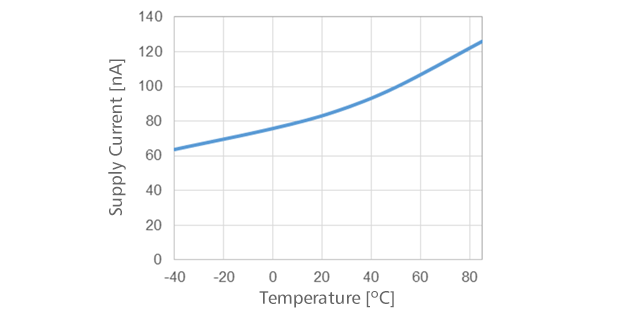
LDO Supply Current vs. Temperature, RP124x18xx, VIN = 2.8 V
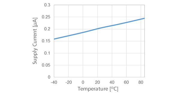
CIN = Ceramic 1.0 µF, COUT = Ceramic 1.0 µF
-
BM Supply Current vs. Temperature, RP124xxx4x, VIN = 3.6 V
CIN = Ceramic 1.0 µF, CBM = Ceramic 0.1 µF
Quality & Packages

- Refer to the datasheets for the details on the product.
- The package file or the datasheet includes package dimensions, taping specifications, taping reels dimensions, power dissipations, and recommended land pattern.
FAQ
Buy / Contact
-
Purchase, Request for samples and documentsSales are made through distributors. Please contact your local distributors for any sales-related inquiry such as price.
-
Available from 1 piece!Our electronic device products are available through our authorized online distributors.
-
Technical Support
RP124 Series