


[Example]
Trouble shooting - Additional LDO solves the problem

Checking circuit itself seemed to be OK, but a trouble is detected! As is often the case with such a trouble, an additional component is used.
Here, the actual trouble shooting example is introduced. It might be useful to choose a device not only for trouble shooting but also just a simple component's selection.
Case 1 Additional LDO solves the problem
LDOs are often used as power management ICs, they are applied to realize constant current circuits, etc.
LDOs are sometimes used for trouble-shooting because they are relatively reasonable cost, the number of external components is only two or less in most cases. How to select the LDO for trouble-shooting is usually same as the normal usage.
Background of the trouble
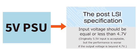
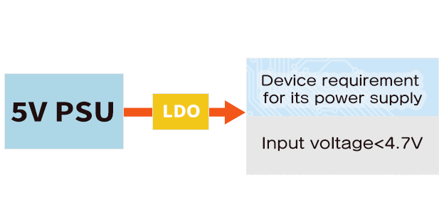
Original circuit: 5V PSU(Power supply unit) directly supplies the power to the post LSI, but the LSI's input voltage is limited up to 4.7V due to keep the post device's characteristics.
The voltage range for the post LSI is relatively wide, but high voltage is better than low voltage for the performance, therefore it is necessary to regulate close to 4.7V.
Cutomer's issue and condition confirmation
To choose the suitable device for this issue, some factors should be considered.
| Check points | Check points list |
|---|---|
| PSU's voltage tolerance: According to the customer 5V±10%. By this information, the input voltage of the regulation device must accept the range from 4.5V to 5.5V. | Input voltage range |
| The target output voltage is less than input voltage, therefore, as the regulation device, an LDO is suitable. The output voltage of LDO has also its tolerance, therefore set output voltage should be less than 4.6V or around. | Acceptable output voltage range |
| In this case, the minimum input voltage is 4.5V. Therefore, if the output voltage of LDO is more than the input voltage, by the load of the post device, output voltage becomes lower than the target output voltage. We should check the fact is acceptable or not. The drop voltage depends on the output current. According to the customer, the maximum output current is 100mA. | Output current (Load current) |
| How about the PCB mount area space? In this case, the space is enough, but small size is better to add the device, however, they do not want to choose leadless type package. | PCB space |
| PCB: 4-layer FR4, internal derating rule: 50% Maximum ambient temperature: 85℃ | Power dissipation |
Trouble shooting Process
According to the information from the customer, part #can be sorted out. Input voltage, Output voltage and output current are the key factors.
1. Input voltage and output current/output voltage
- The maximum output current is 100mA
- Input voltage range 4.5V to 5.5V
- Output voltage candidate 4.4V/4.5V/4.6V
2. Confirm the dropout voltage
Generally, small dropout voltage is better, considering this point, the device candidate is the RP130x Series.
Output voltage candidates are 4.4V/4.5V/4.6V.
The dropout voltage is designated at 150mA. By recalculating 100mA, the result is as follows:
- Typ. 0.24V@150mA-> 0.16V@100mA
- Worst(85℃)0.370V@150mA→0.247V@100mA
| Symbol | Item | Conditions | Typ. | Max. | Unit | |
| VDIF | Dropout Voltage | IOUT = 150 mA | 1.2 V ≤ VSET < 1.5 V | 0.67 | 1 | V |
| 1.5 V ≤ VSET < 1.7 V | 0.54 | 0.81 | ||||
| 1.7 V ≤ VSET < 2.0 V | 0.46 | 0.68 | ||||
| 2.0 V ≤ VSET < 2.5 V | 0.41 | 0.6 | ||||
| 2.5 V ≤ VSET < 4.0 V | 0.32 | 0.51 | ||||
| 4.0 V ≤ VSET | 0.24 | 0.37 | ||||
The minimum input voltage for this customer is 4.5V. By this data, the lowest DC voltage is estimated as Typ. 4.34V, Min. 4.253V. (Not including the transient response) In the original circuit, unregulated input is used, therefore, this drop level can be accpeted as the worst case by the customer, as a result, the customer choose 4.6V output type.
3. Package Selection
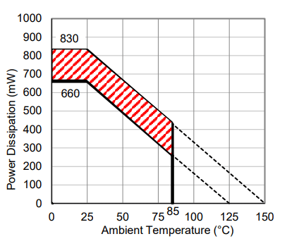
Power Dissipation vs. Ambient Temperature
For package selection, power dissipation must be considered. For this case, the worst condition is as follows: LDO input voltage=5.5V, Output voltage=4.6V (Precisely, torelance is 1%, and load regulation exists, but here, this value is not a big impact on the result, so the rough calculation is shown below)
The power loss is calculated approximately 90mW (5.5V-4.6V)x0.1A=0.09W(90mW)
Derating by 50% should be considered, therefore, power dissipation must be more than 180mW @85℃, 4layer PCB, not leadless type.
As a result, the final candidate is SOT23-5 package RP130N461B-TR-FE (Power dissipation depends on the board material, the number of layers of PCB and via holes, metal area size, and layout.)
4. Other options
The RP130N series have the option of auto-discharge function at off state. In the case shown above, the customer didn't care the point. For this kind of case, popular option is better to choose, so please ask our distributers or sales if possible.
Trouble shooting
- Additional LDO solves the problem
- Additional LDO solves the problem
Trouble was solved with using an additonal LDO, the RP130N461B-TR-FE.
How to select the adittional components for trouble-shooting is similar to how to select the ordinal components at usual design. By considering all necessary conditions such as Vin, Vout, Iout, Power dissipation of the package, trouble shooting could be perfect.